
- Catalogs
- STMicroelectronics
- L4989D, L4989MD

- Products
- Catalogs
- News & Trends
- Exhibitions
L4989D, L4989MD

L4989D, L4989MD
- AEC-Q100 qualified for automotive use.
- Operating voltage range: 5.6 V to 31 V.
- Low quiescent current with optional watchdog disable.
- Precision output voltage with ±3% tolerance.
- Low dropout voltage of 180 mV at 150 mA.
- Reset circuit senses output voltage down to 1 V.
- Programmable reset delay and watchdog timer via external capacitors.
- Thermal shutdown and short circuit protection.
- Temperature range: -40°C to 150°C.
- Maximum DC supply voltage: 40 V; junction temperature: -40 to 150°C.
- Thermal resistance: 50°C/W to 180°C/W based on package and heat sink.
- Output voltage: 4.85 V to 5.15 V under specified conditions.
- Current consumption: 69 µA to 2 mA depending on watchdog and load current.
- Uses a p-channel MOS transistor for low dropout regulation.
- Reset circuit provides a signal if output voltage drops below threshold.
- Watchdog monitors microcontroller, generating reset if pulses are missing; timing adjustable via external capacitor.
- Available in SO-8 and SO-20 packages, ECOPACK® compliant.
- Mechanical dimensions and packing details provided for both packages.
- SO-8 Package: Height: 1.75 mm, Width: 5.80-6.20 mm, Length: 4.80-5.00 mm.
- SO-20 Package: Height: 2.35-2.65 mm, Width: 7.40-7.60 mm, Length: 12.60-13.00 mm.
- SO-8 Packing: Tube: 100 base, 2000 bulk; Tape & Reel: 2500 base and bulk.
- SO-20 Packing: Tube: 40 base, 800 bulk; Tape & Reel: 1000 base and bulk.
- Initial Release: 16-Apr-2012, replacing L4989 datasheet.
- Update: 19-Sep-2013, disclaimer updated.
- Latest Revision: 01-Oct-2018, title updated, "AEC-Q100 qualified" feature added.
Catalog excerpts

L4989D, L4989MD Automotive low power voltage regulator Datasheet - production data Description The L4989M and L4989MD are monolithic integrated 5 V voltage regulators with a low drop voltage at currents up to 150 mA. The output voltage regulating element consists in a p-channel MOS and the regulation is performed regardless of input voltage transients up to 40 V. The high precision of the output voltage is obtained with a pre-trimmed reference voltage. The devices are protected against short circuit and an overtemperature protection switches off the devices in case of extremely high power dissipation. Features AEC-Q100 qualified Operating DC supply voltage range 5.6 V to 31 V The L4989M and L4989MD watchdogs are active when the Enable pin is high. Features like reset and watchdog make this devices particularly suitable to supply microprocessor systems in automotive applications. Very low quiescent current with watchdog disabled Precision output voltage (±3%) Low drop voltage (180 mV typ at Io = 150 mA) Reset circuit sensing the output voltage down to 1 V Programmable reset delay with external capacitor Watchdog disable input Programmable watchdog timer with external capacitor Thermal shutdown and short circuit protection Wide temperature range (Tj = -40°C to 150°C) Table 1. Device summary Order codes Package Tube Tape & reel October 2018 This is information on a product in full production.
Open the catalog to page 1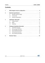
Block diagram and pin configuration . . . . . . . . . . . . . . . . . . . . . . . . . . . 5 Absolute maximum ratings . . . . . . . . . . . . . . . . . . . . . . . . . . . . . . . . . . . . . 7 Electrical characteristics . . . . . . . . . . . . . . . . . . . . . . . . . . . . . . . . . . . . . . . 8 Voltage regulator . . . . . . . . . . . . . . . . . . . . . . . . . . . . . . . . . . . . . . . . . . . .11 Watchdog . . . . . . . . . . . . . . . . . . . . . . . . . . . . . . . . . . . . . . . . . . . . . . . . . 12 Package and packing information . . . . . . . . . . . . . . . . . . . . . . . . ....
Open the catalog to page 2
List of tables Table 1. Table 2. Table 3. Table 4. Table 5. Table 6. Table 7. Table 8. Table 9. Table 10. Table 11. Device summary . . . . . . . . . . . . . . . . . . . . . . . . . . . . . . . . . . . . . . . . . . . . . . . . . . . . . . . . . . 1 Pins description . . . . . . . . . . . . . . . . . . . . . . . . . . . . . . . . . . . . . . . . . . . . . . . . . . . . . . . . . . 5 Absolute maximum ratings . . . . . . . . . . . . . . . . . . . . . . . . . . . . . . . . . . . . . . . . . . . . . . . . . . 7 Thermal data. . . . . . . . . . . . . . . . . . . . . . . . . . . . . . . . . . . . . ....
Open the catalog to page 3
List of figures Figure 1. Figure 2. Figure 3. Figure 4. Figure 5. Figure 6. Figure 7. Figure 8. Figure 9. Figure 10. Figure 11. Block diagram . . . . . . . . . . . . . . . . . . . . . . . . . . . . . . . . . . . . . . . . . . . . . . . . . . . . . . . . . . . . 5 Pins configuration (top view). . . . . . . . . . . . . . . . . . . . . . . . . . . . . . . . . . . . . . . . . . . . . . . . . 6 Behavior of output current versus regulated voltage Vo . . . . . . . . . . . . . . . . . . . . . . . . . . . 11 Reset timing diagram . . . . . . . . . . . . . . . . . . . . . . . . . . . . . . . . . . . . ....
Open the catalog to page 4
Block diagram and pin configuration Block diagram and pin configuration Figure 1. Block diagram Table 2. Pins description Pin name Watchdog Enable input If high watchdog functionality is active. Ground reference Ground. Connected these pins to a heat spreader ground Reset output. It is pulled down when output voltage goes below Vo_th or frequency at Wi is too low. Reset timing adjust. A capacitor between Vcr pin and gnd, sets the reset delay time (trd) Watchdog timer adjust A capacitor between Vcw pin and gnd, sets the time response of the watchdog monitor. Watchdog input. If the frequency at...
Open the catalog to page 5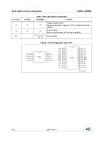
Block diagram and pin configuration Table 2. Pins description (continued) Pin name Voltage regulator output Block to ground with a capacitor >100 nF (needed for regulator stability) Supply voltage Block to ground directly at IC pin with a capacitor Figure 2. Pins configuration (top view)
Open the catalog to page 6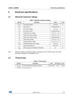
Electrical specifications Electrical specifications Absolute maximum ratings Table 3. Absolute maximum ratings Symbol Input current Internally limited Watchdog input voltage Open Drain output voltage Open Drain output current Internally limited Reset delay voltage Watchdog delay voltage Watchdog Enable input voltage Junction temperature Internally limited ESD voltage level (HBM-MIL STD 883C) Maximum ratings are absolute ratings; exceeding any one of these values may cause permanent damage to the integrated circuit. Thermal data Table 4. Thermal data Symbol Rth-jamb Parameter Thermal resistance...
Open the catalog to page 7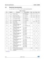
Electrical specifications Electrical characteristics VS = 5.6 V to 31 V, Tj = -40°C to +150°C unless otherwise specified. Table 5. General Test condition Output voltage Short circuit current Output current limitation Line regulation voltage Load regulation voltage Drop voltage Ripple rejection Current consumption with watchdog not active Iqs_1 = IVS-Io Current consumption with watchdog not active Iqs_10 = IVS-Io Current consumption with watchdog not active Iqs_50 = IVS-Io Current consumption with watchdog not active Iqs_150 = IVS-Io Current consumption with watchdog active Iqn_1 = IVS-Io Current...
Open the catalog to page 8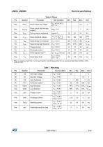
Electrical specifications Table 6. Reset Reset output low voltage Reset output high leakage current Pull up internal resistance Reset threshold voltage Below Vo_ref Reset timing low threshold Reset timing high threshold Charge current Discharge current Reset reaction Test condition Reset delay time 1. When Vo becomes lower than 4 V, the reset reaction time decreases down to 2 µs assuring a faster reset condition in this particular case. Test condition Input high voltage Input hysteresis Pull down resistor High threshold Charge current Discharge current Watchdog period Watchdog output low time
Open the catalog to page 9
Electrical specifications L4989D, L4989MD Table 8. Watchdog Enable Enable input low voltage Enable input high voltage Enable input hysteresis Pull down current Test condition
Open the catalog to page 10All STMicroelectronics catalogs and technical brochures
 STGW30NC60KD
14 Pages
 STGB14NC60K STGD14NC60K
16 Pages
 HD1750FX
8 Pages
 TDA75610SLV
42 Pages
 TDA7391
13 Pages
 TDA7376B
15 Pages
 TDA7375V
15 Pages
 TDA2005
25 Pages
 L4938ED L4938EPD
20 Pages
 L4949ED-E L4949EP-E
19 Pages
 L4925
L492514 Pages
 FDA903U
80 Pages
 FDA803U
76 Pages
 FDA903D
82 Pages
 FDA803D
78 Pages
 BALF-SPI2-02D3
13 Pages
 LIS2DTW12
65 Pages
 VL53L0X
40 Pages
 LPS22HH
59 Pages
 Standard products offer overview
13 Pages
 M40SZ100W
20 Pages
 A1C15S12M3
17 Pages
 TSX923
32 Pages
 TS1851
24 Pages
 LMV321
17 Pages
 Serial real-time clock (RTC) ICs
16 Pages
 TDA2003LG
8 Pages
 HCF4541 Programmable Timer
10 Pages
 STA8058 GPS multi-chip module
14 Pages
 TDA7410ND Signal Processor
34 Pages
 TDA7410ND Signal Processor
34 Pages
 TSA1204 DUAL CHANNEL
31 Pages


Archived catalogs
 NEATSwitch
6 Pages
 Power MOSFETs for metering
2 Pages


- Single-pole switch
- Acceleration sensor
- Pressure probe
- Technology switch
- Piezoelectric accelerometer
- Signal amplifying integrated circuit
- Multipole switch
- Transceiver module
- Electronic filter
- Electromechanical switch
- Membrane pressure sensor
- Rotary electric switch
- Analog pressure sensor
- Triaxial acceleration sensor
- Power amplifying integrated circuit
- Distance sensor
- Diode
- Low-pass electronic filter
- Absolute pressure sensor