- Catalogs
- STMicroelectronics
- L4949ED-E L4949EP-E
L4949ED-E L4949EP-E
1 /19Pages

L4949ED-E L4949EP-E
1 /19Pages
Catalog excerpts

L4949ED-E L4949EP-E Automotive multifunction very low drop voltage regulator Datasheet - production data Description The L4949ED-E and L4949EP-E are monolithic integrated 5V voltage regulators with a very low dropout output and additional functions as poweron reset and input voltage sense. They are designed for supplying the microcomputer controlled systems especially in automotive applications. Features AEC-Q100 qualified ECOPACK®: lead free and RoHS compliant Operating DC supply voltage range 5 V - 28 V Transient supply voltage up to 40 V Extremely low quiescent current in standby High precision standby output voltage 5V±1% Output current capability up to 100 mA Very low dropout voltage less than 0.5 V Reset circuit sensing the output voltage Programmable reset pulse delay with external capacitor Voltage sense comparator Thermal shutdown and short circuit protections Table 1. Device summary Order codes Package Tube September 2018 This is information on a product in full production.
Open the catalog to page 1
Block diagram and pin description . . . . . . . . . . . . . . . . . . . . . . . . . . . . 5 Absolute maximum ratings . . . . . . . . . . . . . . . . . . . . . . . . . . . . . . . . . . . . . 7 Supply voltage transient . . . . . . . . . . . . . . . . . . . . . . . . . . . . . . . . . . . . . 10 Package and packing information . . . . . . . . . . . . . . . . . . . . . . . . . . . . . 15 4.1 4.2
Open the catalog to page 2
List of tables Table 1. Table 2. Table 3. Table 4. Table 5. Table 6. Table 7. Table 8. Table 9. Table 10. Table 11. Device summary . . . . . . . . . . . . . . . . . . . . . . . . . . . . . . . . . . . . . . . . . . . . . . . . . . . . . . . . . . 1 Pin definitions and functions . . . . . . . . . . . . . . . . . . . . . . . . . . . . . . . . . . . . . . . . . . . . . . . . . 6 Absolute maximum ratings . . . . . . . . . . . . . . . . . . . . . . . . . . . . . . . . . . . . . . . . . . . . . . . . . . 7 Thermal data. . . . . . . . . . . . . . . . . . . . . . . . . . . . . . . . . . . . . . . . ....
Open the catalog to page 3
List of figures Figure 1. Figure 2. Figure 3. Figure 4. Figure 5. Figure 6. Figure 7. Figure 8. Figure 9. Figure 10. Block diagram . . . . . . . . . . . . . . . . . . . . . . . . . . . . . . . . . . . . . . . . . . . . . . . . . . . . . . . . . . . . 5 Configuration diagram (top view) . . . . . . . . . . . . . . . . . . . . . . . . . . . . . . . . . . . . . . . . . . . . . 5 Application circuit . . . . . . . . . . . . . . . . . . . . . . . . . . . . . . . . . . . . . . . . . . . . . . . . . . . . . . . . 10 Foldback characteristic of VO . . . . . . . . . . . . . . . . . . . . . . . . . . . ....
Open the catalog to page 4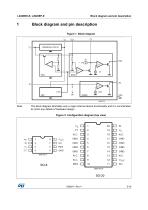
Block diagram and pin description Block diagram and pin description Figure 1. Block diagram The block diagram illustrates only a major internal device functionality and it is not intended to mimic any details of hardware design Figure 2. Configuration diagram (top view)
Open the catalog to page 5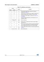
Block diagram and pin description L4949ED-E, L4949EP-E Table 2. Pin definitions and functions Input supply voltage. Block to GND via an external capacitor (see Figure 3). Sense input pin to supervise input voltage. Connect via an external voltage divider connected to VS and to GND. Preregulator output voltage. For details, see Section 3.4: Preregulator. Reset pulse delay adjustment. Connecting this pin via a capacitor to GND Ground reference Reset output. It is pulled down when the output voltage goes below VRT. Sense output. This open collector pin must be connected to VOUT via an external resistor....
Open the catalog to page 6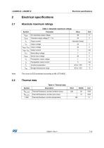
Electrical specifications Electrical specifications Absolute maximum ratings Table 3. Absolute maximum ratings Symbol DC operating supply voltage Transient supply voltage (T < 1s) Output current Internally limited Output voltage VRES, VSO Output voltage Output current Reset delay voltage Sense input voltage Preregulator output voltage Preregulator output current Junction temperature Storage temperature range The circuit is ESD protected according to MIL-STD-883C. Thermal data Table 4. Thermal data Symbol Thermal Resistance Junction-ambient (max) Thermal Shutdown Junction temperature Thermal Resistance...
Open the catalog to page 7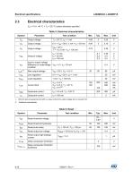
Electrical specifications Electrical characteristics VS = 14 V; -40 °C < Tj < 125 °C unless otherwise specified Table 5. Electrical characteristics Symbol Test condition Output voltage Output voltage Output voltage Dropout voltage Input to output voltage difference in undervoltage VIN = 4 V, IO = 35 mA condition Line regulation Load regulation Current limit ILIM IQSE Quiescent current Quiescent current 1. With this test we guarantee that with no output current the output voltage will not exceed 5.5V 2. Foldback characteristic Table 6. Reset Symbol Reset threshold voltage Test condition Reset...
Open the catalog to page 8
Electrical specifications Table 7. Sense Test condition Sense threshold hysteresis Sense output low voltage Sense output leakage Sense input current Table 8. Preregulator Symbol Preregulator output voltage Test condition Preregulator output current
Open the catalog to page 9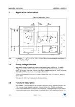
Application information Application information Figure 3. Application circuit For stability: CS 1µF, CO 4.7µF, ESR < 10 at 10KHz. Recommended for application: CS = CO = 10 µF to 100 µF Supply voltage transient High supply voltage transients can cause a reset output signal disturbance. For supply voltages greater than 8V the circuit shows a high immunity of the reset output against supply transients of more than 100V/µs. For supply voltages less than 8V supply transients of more than 0.4V/µs can cause a reset signal disturbance. To improve the transient behaviour for supply voltages less...
Open the catalog to page 10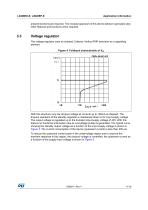
Application information present functions are required. The modular approach of this device allows to get easily also other features and functions when required. Voltage regulator The voltage regulator uses an Isolated Collector Vertical PNP transistor as a regulating element. Figure 4. Foldback characteristic of VO With this structure very low dropout voltage at currents up to 100mA is obtained. The dropout operation of the standby regulator is maintained down to 3V input supply voltage. The output voltage is regulated up to the transient input supply voltage of 40V. With this feature no functional...
Open the catalog to page 11All STMicroelectronics catalogs and technical brochures
 STGW30NC60KD
14 Pages
 STGB14NC60K STGD14NC60K
16 Pages
 HD1750FX
8 Pages
 TDA75610SLV
42 Pages
 TDA7391
13 Pages
 TDA7376B
15 Pages
 TDA7375V
15 Pages
 TDA2005
25 Pages
 L4989D, L4989MD
19 Pages
 L4938ED L4938EPD
20 Pages
 L4925
L492514 Pages
 FDA903U
80 Pages
 FDA803U
76 Pages
 FDA903D
82 Pages
 FDA803D
78 Pages
 BALF-SPI2-02D3
13 Pages
 LIS2DTW12
65 Pages
 VL53L0X
40 Pages
 LPS22HH
59 Pages
 Standard products offer overview
13 Pages
 M40SZ100W
20 Pages
 A1C15S12M3
17 Pages
 TSX923
32 Pages
 TS1851
24 Pages
 LMV321
17 Pages
 Serial real-time clock (RTC) ICs
16 Pages
 TDA2003LG
8 Pages
 HCF4541 Programmable Timer
10 Pages
 STA8058 GPS multi-chip module
14 Pages
 TDA7410ND Signal Processor
34 Pages
 TDA7410ND Signal Processor
34 Pages
 TSA1204 DUAL CHANNEL
31 Pages


Archived catalogs
 NEATSwitch
6 Pages
 Power MOSFETs for metering
2 Pages


- Single-pole switch
- Acceleration sensor
- Pressure probe
- Technology switch
- Signal amplifying integrated circuit
- Multipole switch
- Piezoelectric accelerometer
- Transceiver module
- Electronic filter
- Electromechanical switch
- Analog pressure sensor
- Membrane pressure sensor
- Rotary electric switch
- Triaxial acceleration sensor
- Power amplifying integrated circuit
- Distance sensor
- Diode
- Low-pass electronic filter
- Absolute pressure sensor