L4925
1 /14Pages

L4925
1 /14Pages
Catalog excerpts

L4925 Very low drop voltage regulator Features ■ Operating DC supply voltage range 6 V to 28 V Transient supply voltage up to 40 V Extremely low quiescent current High precision output voltage Output current capability up to 500 mA Very low dropout voltage less than 0.6 V Reset circuit sensing the output voltage Programmable reset pulse delay with external capacitor Thermal shutdown and short circuit protections Description The L4925 is a monolithic integrated 5 V voltage regulator with a very low dropout output and additional functions such as power-on reset and programmable reset delay time. It is designed for supplying microcomputer controlled systems especially in automotive applications. Table 1. Device summary Order codes Package Tube PowerSO-20
Open the catalog to page 1
Block and pin connections diagrams . . . . . . . . . . . . . . . . . . . . . . . . . . . 5 1.1 Absolute maximum ratings . . . . . . . . . . . . . . . . . . . . . . . . . . . . . . . . . . . . . 6 Electrical characteristics . . . . . . . . . . . . . . . . . . . . . . . . . . . . . . . . . . . . . . . 6 Voltage regulator . . . . . . . . . . . . . . . . . . . . . . . . . . . . . . . . . . . . . . . . . . . . 8 Reset circuit . . . . . . . . . . . . . . . . . . . . . . . . . . . . . . . . . . . . . . . . . . . . . . . . 9 Supply voltage transients . . . . . . . . . . . . . . . . . . . . . . . . ....
Open the catalog to page 2
List of tables Table 2. Table 3. Table 4. Table 5. Thermal data. . . . . . . . . . . . . . . . . . . . . . . . . . . . . . . . . . . . . . . . . . . . . . . . . . . . . . . . . . . . . 5 Absolute maximum ratings . . . . . . . . . . . . . . . . . . . . . . . . . . . . . . . . . . . . . . . . . . . . . . . . . . 6 Electrical characteristics . . . . . . . . . . . . . . . . . . . . . . . . . . . . . . . . . . . . . . . . . . . . . . . . . . . . 6 Document revision history . . . . . . . . . . . . . . . . . . . . . . . . . . . . . . . . . . . . . . . . . . . . . . . . . 13
Open the catalog to page 3
List of figures Figure 1. Figure 2. Figure 3. Figure 4. Figure 5. Figure 6. Figure 7. Figure 8. Figure 9. Block diagram . . . . . . . . . . . . . . . . . . . . . . . . . . . . . . . . . . . . . . . . . . . . . . . . . . . . . . . . . . . . 5 PowerSO-20 pin connections (top view). . . . . . . . . . . . . . . . . . . . . . . . . . . . . . . . . . . . . . . . 5 Foldback characteristics of VO . . . . . . . . . . . . . . . . . . . . . . . . . . . . . . . . . . . . . . . . . . . . . . . 8 Output voltage vs input voltage . . . . . . . . . . . . . . . . . . . . . . . . . . . . . . . . . . . . . . . ....
Open the catalog to page 4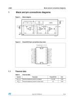
Block and pin connections diagrams Block and pin connections diagrams Figure 1. PowerSO-20 pin connections (top view) Connected to pin 1-10-11-20 Thermal data Table 2. Symbol Rth(j-amb) Rth(j-c) Thermal data Parameter Thermal resistance junction to ambient Thermal resistance junction to case (max)
Open the catalog to page 5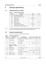
Electrical specifications Electrical specifications Absolute maximum ratings Table 3. Absolute maximum ratings DC operating supply voltage Transient supply voltage (t < 1s) Output current internally limited Output voltage Output voltage Output current Storage temperature Operating junction temperature Thermal shutdown-junction temperature The circuit is ESD protected according to MIL-STD-883C. According to ISO/DIS 7637 the transients must be clamped with external circuitry (see Application Circuit). Electrical characteristics VS =14 V; Tj = –40 to 125 °C unless otherwise specified. Electrical...
Open the catalog to page 6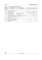
Electrical specifications Electrical characteristics (continued) Parameter Test condition Reset threshold voltage Reset threshold Reset pulse delay Reset reaction time Reset output low voltage Reset output high leakage current Delay comparator threshold Delay comparator threshold hysteresis
Open the catalog to page 7
Functional description Functional description The L4925 is a monolithic integrated voltage regulator, based on the STM modular voltage regulator approach. Several outstanding features and auxiliary functions are implemented to meet the requirements of supplying microprocessor systems in automotive applications. Nevertheless, it is suitable also in other applications where the present functions are required. The modular approach of this device allows to get easily also other features and functions when required. Voltage regulator The voltage regulator uses an Isolated Collector Vertical PNP transistor...
Open the catalog to page 8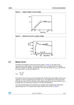
Functional description Figure 4. Output voltage vs input voltage Quiescent current vs supply voltage Reset circuit The block circuit diagram of the reset circuit is shown in Figure 6. The reset circuit supervises the output voltage. The reset threshold of 4.5 V is defined with the internal reference voltage and standby output divider. The reset pulse delay time tRD, is defined with the charge time of an external capacitor CT: C T 2V t RD = ------------------2A The reaction time of the reset circuit originates from the discharge time limitation of the reset capacitor CT and it is proportional...
Open the catalog to page 9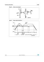
Functional description Block circuit diagram Reset output waveforms
Open the catalog to page 10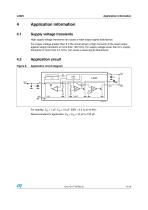
Application information Application information Supply voltage transients High supply voltage transients can cause a reset output signal disturbance. For supply voltage greater than 8 V the circuit shows a high immunity of the reset output against supply transients of more than 100 V/ms. For supply voltage lower than 8 V, supply transients of more than 0.4 V/ms. can cause a reset signal disturbance. Application circuit Application circuit diagram Vo For stability: CS 1 µF; CO 10 µF; ESR 2.5 at 10 KHz Recommended for application: CS = CO = 10 µF to 100 µF
Open the catalog to page 11
Package Informations Package Informations PowerSO-20 mechanical data and package dimensions DIM. OUTLINE AND MECHANICAL DATA (1) “D and E1” do not include mold flash or protusions. - Mold flash or protusions shall not exceed 0.15mm (0.006”) - Critical dimensions: “E”, “G” and “a3”. (2) For subcontractors, the limit is the one quoted in jedec MO-166 SEATING PLANE BOTTOM VIEW
Open the catalog to page 12All STMicroelectronics catalogs and technical brochures
 STGW30NC60KD
14 Pages
 STGB14NC60K STGD14NC60K
16 Pages
 HD1750FX
8 Pages
 TDA75610SLV
42 Pages
 TDA7391
13 Pages
 TDA7376B
15 Pages
 TDA7375V
15 Pages
 TDA2005
25 Pages
 L4989D, L4989MD
19 Pages
 L4938ED L4938EPD
20 Pages
 L4949ED-E L4949EP-E
19 Pages
 FDA903U
80 Pages
 FDA803U
76 Pages
 FDA903D
82 Pages
 FDA803D
78 Pages
 BALF-SPI2-02D3
13 Pages
 LIS2DTW12
65 Pages
 VL53L0X
40 Pages
 LPS22HH
59 Pages
 Standard products offer overview
13 Pages
 M40SZ100W
20 Pages
 A1C15S12M3
17 Pages
 TSX923
32 Pages
 TS1851
24 Pages
 LMV321
17 Pages
 Serial real-time clock (RTC) ICs
16 Pages
 TDA2003LG
8 Pages
 HCF4541 Programmable Timer
10 Pages
 STA8058 GPS multi-chip module
14 Pages
 TDA7410ND Signal Processor
34 Pages
 TDA7410ND Signal Processor
34 Pages
 TSA1204 DUAL CHANNEL
31 Pages


Archived catalogs
 NEATSwitch
6 Pages
 Power MOSFETs for metering
2 Pages


- Single-pole switch
- Acceleration sensor
- Pressure probe
- Technology switch
- Signal amplifying integrated circuit
- Multipole switch
- Piezoelectric accelerometer
- Transceiver module
- Electronic filter
- Electromechanical switch
- Analog pressure sensor
- Membrane pressure sensor
- Rotary electric switch
- Triaxial acceleration sensor
- Power amplifying integrated circuit
- Distance sensor
- Diode
- Low-pass electronic filter
- Absolute pressure sensor