- Catalogs
- STMicroelectronics
- L272 Dual Power Operational Amplifier
L272 Dual Power Operational Amplifier
1 /10Pages

L272 Dual Power Operational Amplifier
1 /10Pages
Catalog excerpts

L272 July 2003 DUAL POWER OPERATIONAL AMPLIFIERS ® ..OUTPUT CURRENT TO 1 A .OPERATES AT LOW VOLTAGES .SINGLE OR SPLIT SUPPLY LARGE COMMON-MODE AND DIFFEREN. TIAL MODE RANGE .GROUND COMPATIBLE INPUTS .LOW SATURATION VOLTAGE THERMAL SHUTDOWN DESCRIPTION The L272 is a monolithic integrated circuits in Powerdip, Minidip and SO packages intended for use as power operational amplifiers in a wide range of applications including servo amplifiers and power supplies, compacts disc, VCR, etc. The high gain and high output power capability provide superior performance whatever an operational amplifier/power booster combination is required. Powerdip (8 + 8) Minidip ORDERING NUMBERS : L272 (Powerdip) L272M (Minidip) L272D (SO16 Narrow) PIN CONNECTIONS (top view) SO16 (Narrow) L272M L272D 1/10
Open the catalog to page 1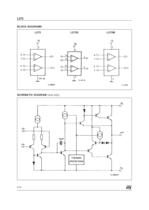
BLOCK DIAGRAMS SCHEMATIC DIAGRAM (one only) L272 L272D L272M L272 2/10
Open the catalog to page 2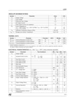
ABSOLUTE MAXIMUM RATINGS Symbol Parameter Value Unit Vs Supply Voltage 28 V Vi Input Voltage Vs Vi Differential Input Voltage ± Vs Io DC Output Current 1 A Ip Peak Output Current (non repetitive) 1.5 A Ptot Power Dissipation at: Tamb = 80°C (L272), Tamb = 50°C (L272M), Tcase = 90 °C (L272D) Tcase = 75 °C (L272) 1.2 5 WW Top Operating Temperature Range (L272D) – 40 to 85 °C Tstg, Tj Storage and Junction Temperature – 40 to 150 °C ELECTRICAL CHARACTERISTICS (VS = 24V, Tamb = 25oC unless otherwise specified) Symbol Parameter Test Conditions Min. Typ. Max. Unit Vs Supply Voltage 4 28 V Is Quiescent...
Open the catalog to page 3
Figure 1 : Quiescent Current versus Supply Voltage Figure 2 : Quiescent Drain Current versus Temperature Figure 3 : Open Loop Voltage Gain Figure 4 : Output Voltage Swing versus Load Current Figure 5 : Output Voltage Swing versus Load Current Figure 6 : Supply Voltage Rejection versus Frequency L272 4/10
Open the catalog to page 4
Figure 7 : Channel Separation versus Frequency Figure 8 : Common Mode Rejection versus Frequency APPLICATION SUGGESTION NOTE In order to avoid possible instability occuring into final stage the usual suggestions for the linear power stages are useful, as for instance : - layout accuracy ; - a 100nF capacitor corrected between supply pins and ground ; - boucherot cell (0.1 to 0.2 mF + 1 W series) between Figure 9 : Bidirectional DC Motor Control with mP Compatible Inputs Figure 10 : Servocontrol for Compact-disc Figure 11 : Capstan Motor Control in Video Recorders L272 5/10
Open the catalog to page 5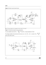
Figure 12 : Motor Current Control Circuit. Note : The input voltage level is compatible with L291 (5-BIT D/A converter). Figure 13 : Bidirectional Speed Control of DC Motors. 2R3 ° R1 For circuit stability ensure that RX > where RM = internal resistance of motor. RM Vs 2R ° R1 The voltage available at the terminals of the motor is VM = 2 (Vi × ) + ½Ro½ × IM where ½Ro½ = 2 RX and IM is the motor current. L272 6/10
Open the catalog to page 6
Information furnished is believed to be accurate and reliable. However, STMicroelectronics assumes no responsibility for the consequences of use of such information nor for any infringement of patents or other rights of third parties which may result from its use. No license is granted by implication or otherwise under any patent or patent rights of STMicroelectronics. Specification mentioned in this publication are subject to change without notice. This publication supersedes and replaces all information previously supplied. STMicroelectronics products are not authorized for use as critical...
Open the catalog to page 10All STMicroelectronics catalogs and technical brochures
 STGW30NC60KD
14 Pages
 STGB14NC60K STGD14NC60K
16 Pages
 HD1750FX
8 Pages
 TDA75610SLV
42 Pages
 TDA7391
13 Pages
 TDA7376B
15 Pages
 TDA7375V
15 Pages
 TDA2005
25 Pages
 L4989D, L4989MD
19 Pages
 L4938ED L4938EPD
20 Pages
 L4949ED-E L4949EP-E
19 Pages
 L4925
L492514 Pages
 FDA903U
80 Pages
 FDA803U
76 Pages
 FDA903D
82 Pages
 FDA803D
78 Pages
 BALF-SPI2-02D3
13 Pages
 LIS2DTW12
65 Pages
 VL53L0X
40 Pages
 LPS22HH
59 Pages
 Standard products offer overview
13 Pages
 M40SZ100W
20 Pages
 A1C15S12M3
17 Pages
 TSX923
32 Pages
 TS1851
24 Pages
 LMV321
17 Pages
 Serial real-time clock (RTC) ICs
16 Pages
 TDA2003LG
8 Pages
 HCF4541 Programmable Timer
10 Pages
 STA8058 GPS multi-chip module
14 Pages
 TDA7410ND Signal Processor
34 Pages
 TDA7410ND Signal Processor
34 Pages
 TSA1204 DUAL CHANNEL
31 Pages


Archived catalogs
 NEATSwitch
6 Pages
 Power MOSFETs for metering
2 Pages


- Single-pole switch
- Acceleration sensor
- Pressure probe
- Technology switch
- Signal amplifying integrated circuit
- Multipole switch
- Piezoelectric accelerometer
- Transceiver module
- Electronic filter
- Electromechanical switch
- Membrane pressure sensor
- Analog pressure sensor
- Rotary electric switch
- Triaxial acceleration sensor
- Power amplifying integrated circuit
- Distance sensor
- Diode
- STMicroelectronics transistor
- Low-pass electronic filter
- Absolute pressure sensor