- Catalogs
- STMicroelectronics
- HD1750FX
HD1750FX
1 /8Pages

HD1750FX
1 /8Pages
Catalog excerpts

HD1750FX HIGH VOLTAGE NPN POWER TRANSISTOR FOR HIGH DEFINITION AND NEW SUPER-SLIM CRT DISPLAYS ■ STATE-OF-THE-ART TECHNOLOGY: DIFFUSED COLLECTOR "ENHANCED GENERATION" EHVS1 WIDER RANGE OF OPTIMUM DRIVE CONDITIONS LESS SENSITIVE TO OPERATING TEMPERATURE VARIATION FULLY INSULATED POWER PACKAGE U.L. COMPLIANT HORIZONTAL DEFLECTION OUTPUT FOR DIGITAL TV, HDTV AND HIGH-END MONITORS Figure 2: Internal Schematic Diagram DESCRIPTION The device is manufactured using Diffused Collector in Planar technology adopting "Enhance High Voltage Structure" (EHVS1) developed to fit High-Definition CRT displays. The new HD product series show improved silicon efficiency bringing updated performance to the Horizontal Deflection stage. Table 1: Order Codes Part Number
Open the catalog to page 1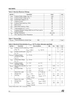
HD1750FX Table 2: Absolute Maximum Ratings Symbol Collector-Emitter Voltage (IB= 0) Emitter-Base Voltage (IC= 0) VEBO IC ICM IB IBM Ptot Vins Tstg TJ Collector Current Collector Peak Current (tp < 5ms) Base Current Base Peak Current (tp < 5ms) Total Dissipation at TC = 25 C Insulation Withstand Voltage (RMS) from All Three Leads to External Heatsink Storage Temperature Max. Operating Junction Temperature Table 3: Thermal Data Rthj-case Thermal Resistance Junction-Case Table 4: Electrical Characteristics (Tcase = 25 oC unless otherwise specified) Symbol ICES Test Conditions Emitter Cut-off Current...
Open the catalog to page 2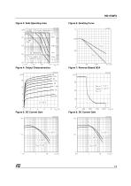
HD1750FX Figure 3: Safe Operating Area Figure 6: Derating Curve Figure 4: Output Chatacterisctics Figure 7: Reverse Biased SOA Figure 5: DC Current Gain Figure 8: DC Current Gain
Open the catalog to page 3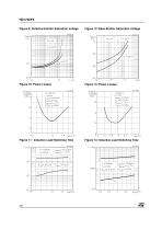
HD1750FX Figure 9: Collector-Emitter Saturation Voltage Figure 12: Base-Emitter Saturation Voltage Figure 10: Power Losses Figure 13: Power Losses Figure 11: Inductive Load Switching Time Figure 14: Inductive Load Switching Time
Open the catalog to page 4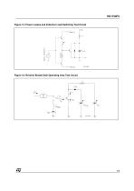
HD1750FX Figure 15: Power Losses and Inductive Load Switching Test Circuit Figure 16: Reverse Biased Safe Operating Area Test Circuit
Open the catalog to page 5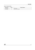
HD1750FX Figure 5: Revision History Release Date Change Designator Initial Release. New hFE value in table 4
Open the catalog to page 7
Information furnished is believed to be accurate and reliable. However, STMicroelectronics assumes no responsibility for the consequences of use of such information nor for any infringement of patents or other rights of third parties which may result from its use. No license is granted by implication or otherwise under any patent or patent rights of STMicroelectronics. Specifications mentioned in this publication are subject to change without notice. This publication supersedes and replaces all information previously supplied. STMicroelectronics products are not authorized for use as critical...
Open the catalog to page 8All STMicroelectronics catalogs and technical brochures
 STGW30NC60KD
14 Pages
 STGB14NC60K STGD14NC60K
16 Pages
 TDA75610SLV
42 Pages
 TDA7391
13 Pages
 TDA7376B
15 Pages
 TDA7375V
15 Pages
 TDA2005
25 Pages
 L4989D, L4989MD
19 Pages
 L4938ED L4938EPD
20 Pages
 L4949ED-E L4949EP-E
19 Pages
 L4925
L492514 Pages
 FDA903U
80 Pages
 FDA803U
76 Pages
 FDA903D
82 Pages
 FDA803D
78 Pages
 BALF-SPI2-02D3
13 Pages
 LIS2DTW12
65 Pages
 VL53L0X
40 Pages
 LPS22HH
59 Pages
 Standard products offer overview
13 Pages
 M40SZ100W
20 Pages
 A1C15S12M3
17 Pages
 TSX923
32 Pages
 TS1851
24 Pages
 LMV321
17 Pages
 Serial real-time clock (RTC) ICs
16 Pages
 TDA2003LG
8 Pages
 HCF4541 Programmable Timer
10 Pages
 STA8058 GPS multi-chip module
14 Pages
 TDA7410ND Signal Processor
34 Pages
 TDA7410ND Signal Processor
34 Pages
 TSA1204 DUAL CHANNEL
31 Pages


Archived catalogs
 NEATSwitch
6 Pages
 Power MOSFETs for metering
2 Pages


- Single-pole switch
- Acceleration sensor
- Pressure probe
- Technology switch
- Signal amplifying integrated circuit
- Multipole switch
- Piezoelectric accelerometer
- Transceiver module
- Electronic filter
- Electromechanical switch
- Membrane pressure sensor
- Analog pressure sensor
- Rotary electric switch
- Triaxial acceleration sensor
- Power amplifying integrated circuit
- Distance sensor
- Diode
- Low-pass electronic filter
- Absolute pressure sensor