
- Catalogs
- STMicroelectronics
- FDA803D

- Products
- Catalogs
- News & Trends
- Exhibitions
FDA803D

FDA803D
- AEC-Q100 qualified for automotive applications.
- Integrated 108 dB D/A conversion with I2S and TDM digital input support.
- Supports input sampling frequencies of 44.1 kHz, 48 kHz, 96 kHz, and 192 kHz.
- Operates on a wide supply range from 3.3 to 18 V.
- Includes MOSFET power outputs for high output power capability.
- Power limiting function configurable via I2C.
- Comprehensive diagnostics including short to VCC/GND, load detection, and thermal warnings.
- Integrated thermal protection and ESD protection.
- Output power: 1 x 25 W /4 Ω @ 14.4 V, 1 kHz THD = 1% and 1 x 30 W /4 Ω @ 14.4 V, 1 kHz THD = 10%.
- Supports 2 Ω load driving.
- Package: PowerSSO-36 with exposed pad down.
- I2C bus diagnostics for short circuits, open load detection, and thermal warnings.
- DC offset and 'hot spot' detection.
- Clipping detector and integrated thermal protection.
- Legacy mode with four configurable settings.
- Hardware mute pin and power limiter function.
- AM operation mode and noise gating.
- Full I2C bus driving capability with 3.3/1.8 V support.
- I2S bus interface with standard and TDM modes.
- Detailed I2C register and timing information provided.
- Operation Principle: Detects differential DC current offset between output pins OUTP and OUTM. The offset is calculated as IOFFSET = |IOUTP-IOUTM|/2 and compared to a threshold set via I2C bits IB10[4,3].
- Result Communication: Controlled via I2C. Detection starts by setting IB3[3]='1'. Results are communicated by setting DB0[6] and DB0[5] flags.
- Hot Spot Detection: Detects soft shorts to Vcc or Gnd, enhancing robustness against hot spots.
- Function: Detects PWM stage saturation by identifying skipped PWM commutations. Enabled by setting IB5[5,4]='01'.
- Output: Provides output via CDDiag pin and sets flag DB1[0]='1'.
- Levels: Three levels of protection against over-temperature: communication of temperature thresholds, output signal attenuation, and power stage shutdown.
- Thresholds: Temperature thresholds can be reduced by 15°C by setting I2C bit IB12[7].
- Function: Enabled by setting I2C IB9[4]='1'. Resets timer at each Word Select line rising edge. Sends muting command and sets flag DB6[2] upon timeout.
- Function: Permanently enabled. Checks coherence of rising edges on Clock line with I2C configuration. Sets flag DB6[1] if an error is detected.
- AM Operation Mode: Allows selection of PWM switching frequency to avoid EM interference. Includes Low Radiation Function (LRF) to minimize PWM duty cycle.
- Noise Gating: Reduces noise when output signal is at non-audible levels. Enabled by default.
- Dither PWM: Improves EMC performance by modulating PWM period. Suggested for use with In Phase modulation.
- Components: Composed of Clock line, Word Select line, and Serial Data line. Supports various sampling frequencies and data formats.
- Timing Requirements: Detailed timing requirements for I2S interface provided.
- Protocol: Data transmission via SDA and SCL lines. Supports multiple addresses and includes start/stop conditions.
- Writing/Reading Procedures: Describes procedures for writing and reading data, including auto-increment options.
Catalog excerpts

FDA803D 1 x 45 W class D digital input automotive power amplifier with diagnostics, wide voltage operation range for car audio and telematic Datasheet - production data 2 Ω loads driving Power limiting function (configurable through I2C) I2C bus diagnostics: – Short to VCC/GND – Short load and open load detection (also in play mode) – Four thermal warnings DC offset detector (also in play) and 'hot spot' detection Integrated thermal protection Legacy mode ('no I2C' mode), 4 configurable settings I2S and TDM digital input (4/8/16CH TDM) Input sampling frequency: 44.1 kHz, 48 kHz, 96 kHz, 192 kHz Full Short circuit and ESD integrated protections Package: PowerSSO-36 exposed pad down Table 1. Device summary CISPR 25 - Class V (Fourth edition) Order code Very low quiescent current Output lowpass filter included in the feedback allowing outstanding audio performances Tape & reel Wide operating supply range from 3.3 to 18 V, suitable for car radio, telematics and e-call MOSFET power outputs allowing high output power capability – 1 x 25 W /4 Ω @ 14.4 V, 1 kHz THD = 1% – 1 x 30 W /4 Ω @ 14.4 V, 1 kHz THD = 10% May 2018 This is information on a product in full
Open the catalog to page 1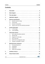
Absolute maximum ratings . . . . . . . . . . . . . . . . . . . . . . . . . . . . . . . . . . . . 13 Typical curves of the main electrical parameters . . . . . . . . . . . . . . . . . . . 17 LC filter design . . . . . . . . . . . . . . . . . . . . . . . . . . . . . . . . . . . . . . . . . . . . . 23 Load possibilities . . . . . . . . . . . . . . . . . . . . . . . . . . . . . . . . . . . . . . . . . . . 23 Finite state machine . . . . . . . . . . . . . . . . . . . . . . . . . . . . . . . . . . . . . . . . 24 7.1 7.2 Diagnostic Vcc-Gnd state . . . . . . . . . . . . . . . . . . . . . . . . . . ....
Open the catalog to page 2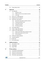
Power limiter control . . . . . . . . . . . . . . . . . . . . . . . . . . . . . . . . . . . . . . . . . 35 Relation with short circuit protection activation . . . . . . . . . . . . . . . . . . . 37 Diagnostic time-line diagrams . . . . . . . . . . . . . . . . . . . . . . . . . . . . . . . . . 38 Open load in play detector . . . . . . . . . . . . . . . . . . . . . . . . . . . . . . . . . . . . 41 11.4.1 Open load in play detector operation overview . . . . . . . . . . . . . . . . . . . 41 Processing bandwidth range . . . . . . . . . . . . . . . . . . . . . . . . . . . . . . . . . 41 Audio signal...
Open the catalog to page 3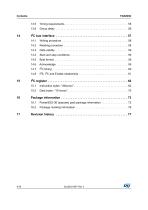
Timing requirements . . . . . . . . . . . . . . . . . . . . . . . . . . . . . . . . . . . . . . . . . 55 Group delay . . . . . . . . . . . . . . . . . . . . . . . . . . . . . . . . . . . . . . . . . . . . . . . 56 Start and stop conditions . . . . . . . . . . . . . . . . . . . . . . . . . . . . . . . . . . . . . 59 Instruction bytes- “I00xxxxx” . . . . . . . . . . . . . . . . . . . . . . . . . . . . . . . . . . . 62 Data bytes - “I01xxxxx” . . . . . . . . . . . . . . . . . . . . . . . . . . . . . . . . . . . . . . . 70 PowerSSO-36 (exposed pad) package information . . . . . . . . . . . . . ....
Open the catalog to page 4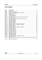
List of tables Table 1. Table 2. Table 3. Table 4. Table 5. Table 6. Table 7. Table 8. Table 9. Table 10. Table 11. Table 12. Table 13. Table 14. Table 15. Table 16. Table 17. Table 18. Table 19. Table 20. Table 21. Table 22. Table 23. Table 24. Table 25. Table 26. Table 27. Table 28. Table 29. Table 30. Table 31. Table 32. Table 33. Table 34.
Open the catalog to page 5
List of figures Figure 1. Figure 2. Figure 3. Figure 4. Figure 5. Figure 6. Figure 7. Figure 8. Figure 9. Figure 10. Figure 11. Figure 12. Figure 13. Figure 14. Figure 15. Figure 16. Figure 17. Figure 18. Figure 19. Figure 20. Figure 21. Figure 22. Figure 23. Figure 24. Figure 25. Figure 26. Figure 27. Figure 28. Figure 29. Figure 30. Figure 31. Figure 32. Figure 33. Figure 34. Figure 35. Figure 36. Figure 37. Figure 38. Figure 39. Figure 40. Figure 41. Figure 42. Figure 43. Figure 44. Figure 45. Figure 46. Figure 47. Figure 48. Block diagram . . . . . . . . . . . . . . . . . . . . . . . . ....
Open the catalog to page 6
Figure 49. Figure 50. Figure 51. Figure 52. Figure 53. Figure 54. Figure 55. Figure 56. Figure 57. Figure 58. Figure 59. Figure 60. Figure 61. Figure 62. Figure 63. Figure 64. Figure 65. Figure 66. Figure 67. Figure 68. Figure 69. Figure 70. Figure 71. Figure 72. Figure 73. Figure 74. DC Diagnostic in Mute . . . . . . . . . . . . . . . . . . . . . . . . . . . . . . . . . . . . . . . . . . . . . . . . . . . . 39 Short circuit protection activation - Short to VCC . . . . . . . . . . . . . . . . . . . . . . . . . . . . . . . . 40 Short Circuit Protection activation due to short across load, short...
Open the catalog to page 7
Description The FDA803D is a single bridge class D amplifier, designed in the most advanced BCD technology, intended for any automotive audio application (car radio, telematics and e-call, noise and tone generators, etc). The FDA803D integrates a high performance D/A converter together with powerful MOSFET outputs in class D, so it is very compact and powerful, moreover reaches outstanding efficiency performances (90%). It has a very wide operating range: it can be operated both with standard car battery levels (5.5-18 V operating, compatible to load dump pulse) and with external step-down generated...
Open the catalog to page 8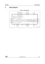
Block diagram Block diagram Figure 1. Block diagram
Open the catalog to page 9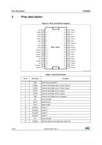
Pins description Pins description Figure 2. Pins connection diagram Table 2. Pins list function Pin # 1 Channel half bridge minus, Power Ground Channel half bridge minus, Power Supply Channel half bridge minus, Output Channel half bridge minus, Output Digital ground Digital supply Device slug connection Channel half bridge minus, Feedback Not connected Clipping detector and diagnostic output pin
Open the catalog to page 10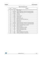
Pins description Table 2. Pins list function Pin # Positive digital supply V(SVR)+0.9V (Internally generated) Negative digital supply V(SVR)-0.9V (Internally generated) test pin, left open I2S/TDM Sync input /Word Select input Analog ground Analog supply Positive Analog Supply V(SVR)+2.5V (Internally generated) Negative Analog Supply V(SVR)-2.5V (Internally generated) Channel half bridge plus, Output Channel half bridge plus, Output Channel half bridge plus, Power Supply Channel half bridge plus, Power Ground Supply Voltage Ripple Rejection Capacitor Hardware mute pin Channel half bridge plus,...
Open the catalog to page 11All STMicroelectronics catalogs and technical brochures
 STGW30NC60KD
14 Pages
 STGB14NC60K STGD14NC60K
16 Pages
 HD1750FX
8 Pages
 TDA75610SLV
42 Pages
 TDA7391
13 Pages
 TDA7376B
15 Pages
 TDA7375V
15 Pages
 TDA2005
25 Pages
 L4989D, L4989MD
19 Pages
 L4938ED L4938EPD
20 Pages
 L4949ED-E L4949EP-E
19 Pages
 L4925
L492514 Pages
 FDA903U
80 Pages
 FDA803U
76 Pages
 FDA903D
82 Pages
 BALF-SPI2-02D3
13 Pages
 LIS2DTW12
65 Pages
 VL53L0X
40 Pages
 LPS22HH
59 Pages
 Standard products offer overview
13 Pages
 M40SZ100W
20 Pages
 A1C15S12M3
17 Pages
 TSX923
32 Pages
 TS1851
24 Pages
 LMV321
17 Pages
 Serial real-time clock (RTC) ICs
16 Pages
 TDA2003LG
8 Pages
 HCF4541 Programmable Timer
10 Pages
 STA8058 GPS multi-chip module
14 Pages
 TDA7410ND Signal Processor
34 Pages
 TDA7410ND Signal Processor
34 Pages
 TSA1204 DUAL CHANNEL
31 Pages


Archived catalogs
 NEATSwitch
6 Pages
 Power MOSFETs for metering
2 Pages


- Single-pole switch
- Acceleration sensor
- Pressure probe
- Technology switch
- Piezoelectric accelerometer
- Multipole switch
- Signal amplifying integrated circuit
- Transceiver module
- Electronic filter
- Electromechanical switch
- Membrane pressure sensor
- Rotary electric switch
- Analog pressure sensor
- Triaxial acceleration sensor
- Distance sensor
- Diode
- STMicroelectronics transistor
- Low-pass electronic filter
- Absolute pressure sensor