- Catalogs
- STMicroelectronics
- EMIF09-SD01F3 Bidirectional 9 line EMI filter + ESD
EMIF09-SD01F3 Bidirectional 9 line EMI filter + ESD
1 /9Pages

EMIF09-SD01F3 Bidirectional 9 line EMI filter + ESD
1 /9Pages
Catalog excerpts

April 2008 Rev 4 1/9 EMIF09-SD01F3 9-line IPAD™, EMI filter and ESD protection Features ¡ 9-line EMI low-pass filter and ESD protection ¡ High efficiency in EMI filtering ¡ Lead-free package ¡ 400 ìm pitch ¡ Very low PCB space occupation: < 4 mm2 ¡ Very thin package: 0.6 mm ¡ High reliability offered by monolithic integration ¡ Reduction of parasitic elements thanks to CSP integration Complies with the following standards ¡ IEC61000-4-2 level 4 on external pins: – 15 kV (air discharge) – 8 kV (contact discharge) ¡ IEC61000-4-2 level 2 on internal pins: – 2 kV (air discharge) – 2 kV (contact discharge) ¡ MIL STD 883F - Method 3015.7 Class 3 Application ¡ Secure digital memory card in mobile phones and communication systems Description The EMIF09-SD01F3 is a highly integrated array designed to suppress EMI/RFI noise for secure digital memory cards. The EMIF09-SD01F3 is in a Flip Chip package to offer space saving and high RF performance. This low-pass filter includes ESD protection circuitry, which prevents damage to the protected device when subjected to ESD surges up 15 kV. This filter also has a low line capacitance to be compatible with high data rate signals. Figure 1. Pin layout (bump side) TM: IPAD is a trademark of STMicroelectronics. Flip Chip 24 bumps A B C D E 5 4 3 2 1 www.st.com
Open the catalog to page 1
Characteristics EMIF09-SD01F3 2/9 1 Characteristics Figure 2. Device configuration GND bumps (GND_H and GND_C - A3, D3 and E3) must be connected to ground on the printed circuit board for ESD testing and RF measurements. Table 1. Pin-signal attribution Pin Description Pin Description Pin Description Pin Description Pin Description A1 DATA2 B1 CD C1 DAT3_PD D1 WP+CD E1 DATA1 A2 DATA3 B2 CMD C2 WP D2 CLK E2 DATA0 A3 GND_H B3 C3 DAT3_PU D3 GND_C E3 GND_C A4 SDDATA2 B4 SDCD C4 SDWP D4 SDWP+CD E4 SDDATA1 A5 SDDATA3 B5 SDCMD C5 VSD D5 SDCLK E5 SDDATA0 Table 2. Absolute ratings (limiting values) Symbol...
Open the catalog to page 2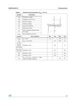
EMIF09-SD01F3 Characteristics 3/9 Table 3. Electrical characteristics (Tamb = 25 °C) Symbol Parameters VBR Breakdown voltage IRM Leakage current @ VRM VRM Stand-off voltage VCL Clamping voltage Rd Dynamic impedance IPP Peak pulse current RI/O Series resistance between input and output Cline Input capacitance per line Symbol Test conditions Min Typ Max Unit VBR IR = 1 mA 6 20 V IRM VRM = 5 V per line 50 200 nA R1, R2, R3, R4, R5, R6, R7, R8, R9 Tolerance ± 20% 40 Ù R11, R12, R13, R14 Tolerance ± 30% 50 kÙ R15 Tolerance ± 30% 15 kÙ R21 Tolerance ± 30% 470 kÙ Cline Vline = 0 V, VOSC = 30 mV, F =...
Open the catalog to page 3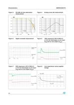
Characteristics EMIF09-SD01F3 4/9 Figure 3. S21(dB) all lines attenuation measurement Figure 4. Analog cross talk measurement 100.0k 1.0M 10.0M 100.0M 1.0G -50.00 data0 data1 data2 data3 -40.00 -30.00 -20.00 -10.00 0.00 F (Hz) dB 100.0k 1.0M 10.0M 100.0M 1.0G -80.00 -70.00 -60.00 -50.00 -40.00 -30.00 -20.00 -10.00 0.00 data0_data1 dB F (Hz) Figure 5. Digital crosstalk measurement Figure 6. ESD response to IEC 61000-4-2 (+15 kV air discharge) on one input (VIN) and on one output (VOUT) Output Line 2 200mV/d Input Line 1 1V/d 10ns/d 5Gs/s Vexternal=20V/d Vinternal=10V/d 100ns/d Figure 7. ESD response...
Open the catalog to page 4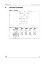
EMIF09-SD01F3 Application information 5/9 2 Application information Figure 9. Aplac model Figure 10. Aplac model variables MODEL = D2 Rline MODEL = D3 Rsub Rbump Lbump MODEL = D1 MODEL = D4 data0 Rbump Lbump sddata0 Rgnd Rbump Lbump Lbump Rbump Lgnd Rgnd Lgnd Rbump Lbump Rgnd Lgnd Variables aplacvar Rline 40 aplacvar C_d1 14.5p aplacvar C_d2 6.5p aplacvar C_d3 303p aplacvar C_d4 14.5p aplacvar Lbump 43pH aplacvar Rbump 17m aplacvar Cbump 150f aplacvar Lgnd 150pH aplacvar Rgnd 10m aplacvar Rsub 5 Diode D1 BV=7 IBV=1m CJO=C_d1 M=0.28 RS=1.13 VJ=0.6 TT=100n Diode D2 BV=7 IBV=1m CJO=C_d2 M=0.28 RS=0.8...
Open the catalog to page 5
Ordering information scheme EMIF09-SD01F3 6/9 3 Ordering information scheme Figure 11. Ordering information scheme 4 Package information In order to meet environmental requirements, ST offers these devices in ECOPACK® packages. These packages have a lead-free second level interconnect. The category of second level interconnect is marked on the inner box label, in compliance with JEDEC Standard JESD97. The maximum ratings related to soldering conditions are also marked on the inner box label. ECOPACK is an ST trademark. ECOPACK specifications are available at www.st.com. Figure 12. Package dimensions...
Open the catalog to page 6
EMIF09-SD01F3 Ordering information 7/9 Figure 15. Flip Chip tape and reel specifications Note: More information is available in the application note: AN2348: “STMicroelectronics 400 micro-metre Flip Chip: Package description and recommendation for use” AN1751: EMI Filters: Recommendations and measurements 5 Ordering information Figure 13. Footprint Figure 14. Marking 220 ìm recommended 220 ìm recommended 260 ìm maximum Solder stencil opening : Copper pad Diameter: Solder mask opening: 300 ìm minimum x y x w z w E Dot, ST logo xx = marking yww = datecode (y = year ww = week) z = manufacturing...
Open the catalog to page 7
Revision history EMIF09-SD01F3 8/9 6 Revision history Table 5. Document revision history Date Revision Changes 19-Oct-2005 1 Initial release. 09-Feb-2006 2 Tape cavity dimensions added in Figure 13. Other graphics improved. 22-Mar-2006 3 Reformatted to current standard. Typical and maximum values updated for IRM in Electrical characteristics, page 3. 28-Apr-2008 4 Updated ECOPACK statement. Updated Figure 11, Figure 12 and Figure 15. Reformatted to current standards.
Open the catalog to page 8
EMIF09-SD01F3 9/9 Please Read Carefully: Information in this document is provided solely in connection with ST products. STMicroelectronics NV and its subsidiaries (“ST”) reserve the right to make changes, corrections, modifications or improvements, to this document, and the products and services described herein at any time, without notice. All ST products are sold pursuant to ST’s terms and conditions of sale. Purchasers are solely responsible for the choice, selection and use of the ST products and services described herein, and ST assumes no liability whatsoever relating to the choice, selection...
Open the catalog to page 9All STMicroelectronics catalogs and technical brochures
 STGW30NC60KD
14 Pages
 STGB14NC60K STGD14NC60K
16 Pages
 HD1750FX
8 Pages
 TDA75610SLV
42 Pages
 TDA7391
13 Pages
 TDA7376B
15 Pages
 TDA7375V
15 Pages
 TDA2005
25 Pages
 L4989D, L4989MD
19 Pages
 L4938ED L4938EPD
20 Pages
 L4949ED-E L4949EP-E
19 Pages
 L4925
L492514 Pages
 FDA903U
80 Pages
 FDA803U
76 Pages
 FDA903D
82 Pages
 FDA803D
78 Pages
 BALF-SPI2-02D3
13 Pages
 LIS2DTW12
65 Pages
 VL53L0X
40 Pages
 LPS22HH
59 Pages
 Standard products offer overview
13 Pages
 M40SZ100W
20 Pages
 A1C15S12M3
17 Pages
 TSX923
32 Pages
 TS1851
24 Pages
 LMV321
17 Pages
 Serial real-time clock (RTC) ICs
16 Pages
 TDA2003LG
8 Pages
 HCF4541 Programmable Timer
10 Pages
 STA8058 GPS multi-chip module
14 Pages
 TDA7410ND Signal Processor
34 Pages
 TDA7410ND Signal Processor
34 Pages
 TSA1204 DUAL CHANNEL
31 Pages


Archived catalogs
 NEATSwitch
6 Pages
 Power MOSFETs for metering
2 Pages


