- Catalogs
- STMicroelectronics
- BALF-SPI2-02D3
BALF-SPI2-02D3
1 /13Pages

BALF-SPI2-02D3
1 /13Pages
Catalog excerpts
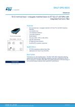
50 Q nominal input / conjugate matched balun to ST S2-LP, 433 MHz with integrated harmonic filter Features • 50 Q nominal input / conjugate matched to ST S2-LP for 433 MHz frequency operation • Low insertion loss • Low amplitude imbalance • Low phase imbalance Flip-Chip (6 bumps) package • Small footprint • Very low profile < 620 pm after reflow • High RF performance • 433 MHz impedance matched balun filter Pinout diagram - Top view Product status Description This device is an ultra-miniature balun. The BALF-SPI2-02D3 integrates matching network and harmonics filter. Matching impedance has been customized for the ST S2-LP transceiver. The BALF-SPI2-02D3 uses STMicroelectronics IPD technology on non-conductive glass substrate which optimize RF performance. DS12508 - Rev 1 - May 2018 For further information contact your local STMicroelectronics sales office.
Open the catalog to page 1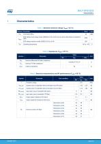
1 Characteristics Table 1. Absolute maximum ratings (Tamb = 25 °C)
Open the catalog to page 2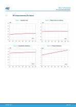
Figure 3. Amplitude imbalance
Open the catalog to page 3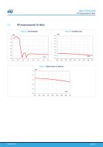
1.2 RF measurements (Tx filter) Figure 5. Transmission 0 (dB)
Open the catalog to page 4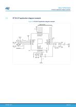
BALF-SPI2-02D3 ST S2-LP application diagram example ST S2-LP application diagram example Figure 8. ST S2-LP application diagram example
Open the catalog to page 5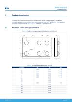
2 Package information In order to meet environmental requirements, ST offers these devices in different grades of ECOPACK® packages, depending on their level of environmental compliance. ECOPACK® specifications, grade definitions and product status are available at: www.st.com. ECOPACK® is an ST trademark. Table 4. Flip-Chip 6 bumps dimensions (in mm)
Open the catalog to page 6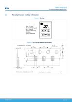
BALF-SPI2-02D3 Flip-chip 6 bumps packing information Flip-chip 6 bumps packing information Figure 10. Marking Dot, ST logo ECOPACK grade xx = marking z = manufacturing location yww = datecode Figure 11. Flip Chip tape and reel specifications Dot identifying Pin All dimensions are typical values in mm User direction of unreeling
Open the catalog to page 7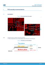
3.1 Land pattern Figure 12. Recommended balun land pattern (*)Clearance 250ym is needed to ensure good sensitivity. (**)1000 ym length between S2-LP & balun (between center QFN pads to center IPD pads). Figure 13. PCB stack-up recommendations Bottom plane 35um + 31 um GND plane
Open the catalog to page 8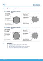
BALF-SPI2-02D3 Stencil opening design Stencil opening design Figure 14. Footprint - 3 mils stencil -non solder mask defined Copper pad diameter: 220 µm recommended 180 µm minimum 260 µm maximum Solder mask opening: 320 µm recommended 300 µm minimum 340 µm maximum Solder stencil opening: 220 µm recommended Figure 16. Footprint - 5 mils stencil -non solder mask defined Copper pad diameter: 220 µm recommended 180 µm minimum 260 µm maximum Solder mask opening: 320 µm recommended 300 µm minimum 340 µm maximum Solder stencil opening: 330 µm recommended* *depending on paste, it can go down to 270 µm...
Open the catalog to page 9
Manual positioning is not recommended. It is recommended to use the lead recognition capabilities of the placement system, not the outline centering Standard tolerance of ±0.05 mm is recommended. 1.0 N placement force is recommended. Too much placement force can lead to squeezed out solder paste and cause solder joints to short. Too low placement force can lead to insufficient contact between package and solder paste that could cause open solder joints or badly centered packages. To improve the package placement accuracy, a bottom side optical control should be performed with a high resolution...
Open the catalog to page 10
4 Ordering information Table 5. Ordering information
Open the catalog to page 11
BALF-SPI2-02D3 Revision history Table 6. Document revision history
Open the catalog to page 12
IMPORTANT NOTICE – PLEASE READ CAREFULLY STMicroelectronics NV and its subsidiaries (“ST”) reserve the right to make changes, corrections, enhancements, modifications, and improvements to ST products and/or to this document at any time without notice. Purchasers should obtain the latest relevant information on ST products before placing orders. ST products are sold pursuant to ST’s terms and conditions of sale in place at the time of order acknowledgement. Purchasers are solely responsible for the choice, selection, and use of ST products and ST assumes no liability for application assistance...
Open the catalog to page 13All STMicroelectronics catalogs and technical brochures
 STGW30NC60KD
14 Pages
 STGB14NC60K STGD14NC60K
16 Pages
 HD1750FX
8 Pages
 TDA75610SLV
42 Pages
 TDA7391
13 Pages
 TDA7376B
15 Pages
 TDA7375V
15 Pages
 TDA2005
25 Pages
 L4989D, L4989MD
19 Pages
 L4938ED L4938EPD
20 Pages
 L4949ED-E L4949EP-E
19 Pages
 L4925
L492514 Pages
 FDA903U
80 Pages
 FDA803U
76 Pages
 FDA903D
82 Pages
 FDA803D
78 Pages
 LIS2DTW12
65 Pages
 VL53L0X
40 Pages
 LPS22HH
59 Pages
 Standard products offer overview
13 Pages
 M40SZ100W
20 Pages
 A1C15S12M3
17 Pages
 TSX923
32 Pages
 TS1851
24 Pages
 LMV321
17 Pages
 Serial real-time clock (RTC) ICs
16 Pages
 TDA2003LG
8 Pages
 HCF4541 Programmable Timer
10 Pages
 STA8058 GPS multi-chip module
14 Pages
 TDA7410ND Signal Processor
34 Pages
 TDA7410ND Signal Processor
34 Pages
 TSA1204 DUAL CHANNEL
31 Pages


Archived catalogs
 NEATSwitch
6 Pages
 Power MOSFETs for metering
2 Pages


- Single-pole switch
- Acceleration sensor
- Pressure probe
- Technology switch
- Signal amplifying integrated circuit
- Multipole switch
- Piezoelectric accelerometer
- Electronic filter
- Electromechanical switch
- Membrane pressure sensor
- Analog pressure sensor
- Rotary electric switch
- Triaxial acceleration sensor
- Power amplifying integrated circuit
- Distance sensor
- Diode
- STMicroelectronics transistor
- Low-pass electronic filter
- Absolute pressure sensor