- Catalogs
- Sony Semiconductors
- Progressive Scan System CCD ICX285AQ
- Products
- Catalogs
- News & Trends
- Exhibitions
Progressive Scan System CCD ICX285AQ

Progressive Scan System CCD ICX285AQ
Catalog excerpts
Description The ICX285AQ is a diagonal 11mm (Type 2/3)interline CCD solid-state image sensor with a squarepixel array. High sensitivity and low smear areachieved through the adoption of EXview HAD CCD technology. Progressive scan allows all pixels'signals to be output independently within approximately1/15 second. Also, the adoption of high frame rate readout mode supports 60 frames per second. Thischip features an electronic shutter with variablecharge-storage time which makes it possible to realize full-frame still images without a mechanical shutter.High resolution and high color reproductively areachieved through the use of R, G, B primary color mosaic filters.This chip is suitable for image input applicationssuch as still cameras which requires high resolution, etc. 20 pin DIP (Ceramic) Features Progressive scan allows individual readout of the image signals from all pixels. ? High horizontal and vertical resolution (both approximately 800 TV-lines) still images without a mechanicalshutter ? Supports high frame rate readout mode(effective 256 lines output, 60 frames/s) ? Square pixel ? Aspect ratio : 4:3 ? Horizontal drive frequency: 28.64MHz ? R, G, B primary color mosaic filters on chip ? High sensitivity, low smear ? Low dark current, excellent anti-blooming characteristics ? Continuous variable-speed shutter function ? Horizontal register: 5.0V drive Device Structure? Interline CCD image sensor > Pin 1 ? Image size:Diagonal 11mm (Type 2/3) Optical black position(Top View) ? Total number of pixels:1434 (H) 1050 (V) approx. 1.50M pixels ? Number of effective pixels:1392 (H) 1040 (V) approx. 1.45M pixels ? Number of active pixels:1360 (H) ח 1024 (V) approx. 1.40M pixels ? Chip size:10.2mm (H) 8.3mm (V) ? Unit cell size:6.45m (H) 6.45m (V) ? Optical black:Horizontal (H) direction:Front 2 pixels, rear 40 pixelsVertical (V) direction:Front 8 pixels, rear 2 pixels > Pin 1140H282V ? Number of dummy bits:Horizontal 20Vertical 3 ? Substrate material:Silicon > ∗ EXview HAD CCD is a trademark of Sony Corporation.EXview HAD CCD is a CCD that drastically improves light efficiency by including near infrared light region as a basic structure ofHAD (Hole-Accumulation-Diode) sensor. 1 ֖ > E01420B3ZSony reserves the right to change products and specifications without prior notice. This information does not convey any license byany implication or otherwise under any patents or other right. Application circuits shown, if any, are typical examples illustrating theoperation of the devices. Sony cannot assume responsibility for any problems arising out of the use of these circuits. size="-1">
Open the catalog to page 1
ICX285AQ USE RESTRICTION NOTICE (December 1, 2003 ver.) This USE RESTRICTION NOTICE ("Notice") is for customers who are considering or currently using the CCDproducts ("Products") set forth in this specifications book. Sony Corporation ("Sony") may, at any time, modifythis Notice which will be available to you in the latest specifications book for the Products. You should abide bythe latest version of this Notice. If a Sony subsidiary or distributor has its own use restriction notice on the Products, such a use restriction notice will additionally apply between you and the subsidiary or distributor....
Open the catalog to page 2
∗ > ICX285AQ Absolute Maximum Ratings ItemV RatingsUnitRemarks > DD , V > OUT , φ RG ֏ SUBV Ə > 2A , V Ə > 2B Ɩ φ SUBV Against φ SUBAgainst φ > 1 , V φ > 3 , V φ > 4 , V > L ֏ SUBH Ə > 1 , H Ə > 2 , GND Ɩ φ SUBC > SUB ֏ SUBV > DD , V > OUT , Ə RG, C > SUB Ɩ GNDV φ GNDAgainst φ > 1 , V φ > 2A , V φ > 2B , V φ > 3 , V φ > 4 GNDH ֏ > 1 , H Ə > 2 Ɩ GNDV φ > 2A , V φ > 2B V > L ֏ V > L V Ə > 1 , V Ə > 3 , V Ə > 4 , H Ə > 1 , H Ə > 2 , GND Ɩ V > L Voltage difference between vertical clock input pinsH > 1 Between inputclock pinsStorage temperatureGuaranteed temperature of performance Operating temperature...
Open the catalog to page 4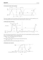
ICX285AQ (3) Horizontal transfer clock waveform > tf φ 2 90%10%H V CR φ H twltwo twhV V φ H 2 trH φ 1 V HL Cross-point voltage for the H φ > 1 rising side of the horizontal transfer clocks H φ > 1 and H φ > 2 waveforms is V > CR .The overlap period for twh and twl of horizontal transfer clocks H φ > 1 and H φ > 2 is two. (4) Reset gate clock waveform > trtwhtwltf V RGH RG waveformV V φ RG Point A RGLH V RGLL V RGL V RGLm V > RGLH is the maximum value and V > RGLL is the minimum value of the coupling waveform during the period fromPoint A in the above diagram until the rising edge of RG. In addition,...
Open the catalog to page 8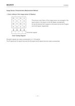
ICX285AQ Image Sensor Characteristics Measurement MethodColor coding of this image sensor & Readout GbBGbBRGrRGrGbBGbBRGrRGr The primary color filters of this image sensor are arranged in thelayout shown in the figure on the left (Bayer arrangement). Gr and Gb denote the G signals on the same line as the R signal and the B signal, respectively. Horizontal register Color Coding Diagram All pixels' signals are output successively in a 1/15s period.The R signal and Gr signal lines and the Gb signal and B signal lines are output successively. 11 ֖ >
Open the catalog to page 11
ICX285AQ Image Sensor Characteristics Measurement MethodMeasurement conditions (1)In the following measurements, the device drive conditions are at the typical values of the bias and clockvoltage conditions, and the progressive scan mode is used.(2)In the following measurements, spot blemishes are excluded and, unless otherwise specified, the opticalblack level (OB) is used as the reference for the signal output, which is taken as the value of the Gr/Gbsignal output or the R/B signal output of the measurement system. Definition of standard imaging conditions (1)Standard imaging condition I :Use...
Open the catalog to page 13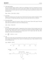
ICX285AQ 4.Video signal shadingSet to the standard imaging condition III . With the lens diaphragm at F5.6 to F8, adjusting the luminousintensity so that the average value of the Gr signal output is 200mV. Then measure the maximum value(Grmax [mV]) and minimum value (Grmin [mV]) of the Gr signal output and substitute the values into the following formula.SHg = (Grmax Grmin) /200 ֗ 100 [%]5.Dark signalMeasure the average value of the signal output (Vdt [mV]) with the device ambient temperature of 60C and the device in the light-obstructed state, using the horizontal idle transfer level as a reference.6.Dark...
Open the catalog to page 14All Sony Semiconductors catalogs and technical brochures
 IMX901-AMR
2 Pages
 IMX490
2 Pages
 IMX290NQV
2 Pages
 ISX016
2 Pages
 IMX390CQV
2 Pages
Archived catalogs
 SLD344YT
6 Pages
 SLD432S
5 Pages
 CXA3314ER
16 Pages
 CXB1818Q
17 Pages
 ICX205AK
24 Pages
 CXA2096N
17 Pages
 SLD433S4
5 Pages
 CXA4416GC
21 Pages
 CXA2984GC SP4T ANT SW
11 Pages
 SLD335YT
5 Pages
 CXM3807K
24 Pages
 CXM3648UR
11 Pages
 CXM3645ER
12 Pages
 CXM3642K
29 Pages
 CXM3641ER
22 Pages
 CXM3632ER
22 Pages
 CXM3630UR
15 Pages
 CXM3617ER
23 Pages
 CXM3614ER
14 Pages
 CXM3604UR
14 Pages
 CXM3599UR
15 Pages
 CXM3593UR
11 Pages
 SLD1332V
5 Pages
 CXM3592AUR
15 Pages
 CXM3583AUR
17 Pages
 CXM3582UR
17 Pages
 CXM3580UR
13 Pages
 CXM3580AUR
17 Pages
 CXM3572ER
14 Pages
 CXM3570ER
13 Pages
 CXM3569XR
13 Pages
 ICX418ALB
20 Pages
 CXD4728R
68 Pages
 ICX642BKA
23 Pages
 CXA3791EN
13 Pages
 SLD332F
6 Pages
 CXG1407XR
11 Pages
 IMX291LQR
2 Pages
 IMX252LLR/LQR
2 Pages
 IMX230
2 Pages
 IMX377CQT
5 Pages
 IMX249LLJ/LQJ
2 Pages
 IMX323LQN
2 Pages
 IMX258
2 Pages
 IMX302LQJ
2 Pages
 CXD4017R
34 Pages
 CXA3197R
30 Pages
 IMX222LQJ
2 Pages
 IMX324
2 Pages
 IMX367LLA
2 Pages
 IMX412-AACK
2 Pages
 IMX385LQR
2 Pages
 IMX294CJK
2 Pages
 IMX253LLR/LQR
2 Pages
 IMX273LLR/LQR
2 Pages
 IMX183CLK-J/CQJ-J
2 Pages
 IMX249LLJ/IMX249LQJ
2 Pages
 IMX250LLR/LQR,IMX252LLR/LQR
2 Pages
 B/W Video Camera CCD ICX422AL
17 Pages
 B/W Video Camera CCD ICX279AL*2
18 Pages
 Color Video Camera CCD ICX239AKE
18 Pages
 Color Video Camera CCD ICX418AKL
22 Pages


- Liebherr display
- LCD display panel
- Color display panel
- LED display panel
- RGB display panel
- Compact display panel
- GNSS receiver
- Compact receiver
- Industrial receiver
- OLED display
- High-definition display module
- Laser diode
- Satellite receiver
- Liebherr CMOS image sensor
- Vision sensor
- Communication card
- Full HD display
- Fiber laser diode
- Codec
- Liebherr visible image sensor