- Catalogs
- Sony Semiconductors
- Optical Communication Transmitter IC CXB1549Q
- Products
- Catalogs
- News & Trends
- Exhibitions
Optical Communication Transmitter IC CXB1549Q

Optical Communication Transmitter IC CXB1549Q
- Maximum data rate of 1.25Gbps (NRZ).
- Automatic Power Control (APC) for bias current management.
- Power on Reset and Activity detector functions for laser safety.
- Signal Duty cycle correction and Power indicate function.
- Differential PECL inputs or AC coupled inputs.
- Supply voltage range: -0.3 to +6.0 V.
- Bias output current: 0 to 80 mA.
- Modulation output current: 0 to 70 mA.
- Operating temperature: -40 to +85 °C.
- Data Buffer: Buffers ECL/PECL data and adds delay to the falling edge of the pulse.
- VBB Generator: Provides reference bias voltage for AC coupling inputs.
- Modulation Current Generator: Sinks up to 50mA for laser diode modulation, with monitoring capability.
- Laser Diode Bias Current Generator: Sources up to 60mA for laser diode biasing, controllable via current or voltage.
- APC Circuitry: Includes window comparator, APC OpAmp, and laser diode alarm circuit for automatic power control.
- Shutdown and Input Alarm Circuitry: Disables modulation and bias currents under specific conditions for safety.
- DC power supply voltage: 3.14 to 3.46 V.
- Power supply current: -76 to -59 mA.
- Modulation output current range: 6 to 50 mA.
- Bias output current range: 0 to 60 mA.
- Activity detector shuts down currents if no data transition is detected.
- Power on Reset holds currents off during system power application.
- Laser diode alarm alerts for abnormal current levels.
Catalog excerpts
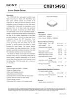
Application? Gbit-ethernet:1.25Gb/s ? SONET/SDH:622Mb/s ? Fibre channel:532Mb/s, 1.062Gb/s Absolute Maximum Ratings? Supply voltageVcc V Features֕ Maximum data rate (NRZ): 1.25Gbps ? Power on Reset function ? Alarm and Shutdown function ? Signal Duty cycle correction ? Automatic Power Control (APC) for bias current ? Activity detector function for laser safety ? Power indicate function ? Differential PECL inputs or AC coupled inputs > Description The CXB1549Q is a high-speed monolithic LaserDiode Driver/Current Switch with ECL/PECL input level. Open collector outputs are provided at the output pins (Q, QBX) and have the capacity of driving modulation current of 50mAp-p at a max. data rate of 1.25Gbps (Min.).Along with the modulation current generator there is the laser diode bias generator which has capacity of sourcing up to 60mA (Bias). The laser diode current can be controlled by either a voltage or current into the bias adjust pin (BiasAdj) and the bias set pin (SBias), depending on how these pins are configured. Control of the diode bias current is achieved through the APC (Automatic Power Control) circuitry. In order to avoid having a large current go through the laser diode, this IC also provides an Activity detector and Power on Reset functions for Laser Safety. The Activity detector circuit detects data edge transitions and if no data transition occur after a certain time period, then both the modulation and bias current are shutdown.The Power on Reset circuit holds the modulationand bias current off for a set period of time while the system power is applied. Additionally, this IC has an internal Duty Cycle correction circuit that can control the falling edge of the input pulse up to a maximum of 0.2ns (Min.). 40 pin QFP (Plastic) > EE 0.3 to +6.0V ? Input voltageV > IN V > EE to VccV ? Differential input voltage| V > D ֖ V > DB |0 to 2.5V ? Bias output current0 to 80mA ? Modulation output current0 to 70mA ? SBias input/output current0 to 5mA ? Input bias control currentIset (Ibiasadj)0 to 5mA ? Input bias control voltageVset (Vbiasadj)0 to 3V ? Storage temperatureTstg65 to +150ְC Recommended Operating Conditions? DC power supply voltageVcc V > EE 3.14 to 3.46V ? Operating ambient temperatureTa֖40 to +85C Structure Bipolar silicon monolithic ICЖ 1 > E98313C0Z-PSSony reserves the right to change products and specifications without prior notice. This information does not convey any license byany implication or otherwise under any patents or other right. Application circuits shown, if any, are typical examples illustrating theoperation of the devices. Sony cannot assume responsibility for any problems arising out of the use of these circuits. size="-1">
Open the catalog to page 1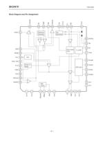
2DDBV 2 QV BB CC EE LDAlmB RS RSB Tset Indicate V V 30 29 28 27 26 25 24 23 22 21 31 ReferenceGenerator V > BB Generator 20ADCDis 19TM 32 18NC Duty CycleCont In_ALM 33 17Timer > REF 34 V > REF 16CompB TEST_PINSDNBSDN LDAlm 35 > CC 3V 36 Power onReset 15CompA DRV Cont 37 14DrvAdj > EE 3CapZV 38V 13 39APCOut 40RsetPD 12V > EE 1 Bias Circuit 11V > CC 1 1 2 3 4 5 6 7 8 9 10 DrvMon > 4 4 5BiasSBias V 1 1 EE EE EE EE CC QBX V V V BiasAdj
Open the catalog to page 2
CXB1549Q Pin Description PadNo.1V > CC 43.3Positive power supplypin for APC circuit.2V > EE 40Negative power supplypin for APC circuit. 6V > V CC 4 5 3 308 10pF240 V EE EE 50Negative power supplypin for Bias circuit.7Q1.3 to 3.36mA to 30mA ∗ > 1 7 8 Laser modulationcurrent output pin. Open collector output. 9, 10V 6mA to 50mA ∗ > 2 ∗ > 1 8QBX1.3 to 3.36mA to 30mA > CurrentSource 6mA to 50mA ∗ > 2 V EE EE 10Negative power supplypin for Driver circuit.11V > CC 13.3Positive power supplypin for Driver circuit.12V > EE 10Negative power supplypin for Driver circuit.13DrvMon0Ato600յASets Laser modulationcurrent...
Open the catalog to page 3
CXB1549Q Description of each function block1. Data Buffer 2. V Data Buffer is comprised of the data buffer and delay generator. ECL/PECL data is input to the data buffer at a maximum data rate of 1.25Gbps. This data is buffered and input to the delay circuitry. The delay circuitry adds a delay to the falling edge of the pulse up to a maximum of 0.2ns (Min.). The delay is set by a single external resistor between the delay set pin (Tset-Pin 27) and Vcc. A plot of the high pulse width vs. set resistance (Rset) is shown in Fig. 1. 5. APC (Automatic Power Control) Circuitry The APC Circuitry is comprised...
Open the catalog to page 10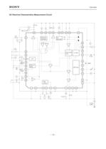
32 18 Duty CycleCont In_ALM 33 17 F 3.14 to 3.46V >
Open the catalog to page 12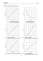
[mA] Q I Falling edge delay [ns] 00.4֖0.3 0.2֖0.10 0.40.30.20.1 1234Rset [k 5678 0020103040 5060 24Rdrv [k > s] s] յ Shutdown time [ Power on time [100 0.510302040506070 12Ctimer [nF] 341.52.53.54.5 00.00.5 1.01.52.0 24Cap_Z [nF] 6810 >
Open the catalog to page 15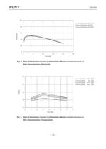
CXB1549Q I > Q /I > DRVMON (A) 3.14V I > Q /I > DRVMON (A) 3.3V I > Q /I > DRVMON (A) 3.46V > DRVMON /I Q I R > ADJ [k Ω ]00204060 80100 510152025 >
Open the catalog to page 16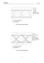
CXB1549Q V > CC = 0V V > EE = 3.3VRL = 25 ֢Ħ Ta = 27 CIQ = 30mA Single input Pattern = PRBS2 > 23 Ж 1Data Rate 1.25Gbps Ch.1 :150mV/div, Offset: 300mV Bandwidth: 20.0GHz Time Base : 200ps/div > 2 V > CC = 0V V > EE = ֖3.3VFPLD ( ֎ = 1330nm)Ta = 27 ۰ CSingle Input Pattern = PRBS2 > 23 1Data Rate 1.06Gbps Filter (Cut Off 700Mbps) Mask: FC1063Ch.2 :5.0mV/div, Offset: 12.8mV Bandwidth: 12.4GHz Time Base:200ps/div 31 >
Open the catalog to page 17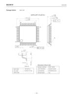
DETAIL A PACKAGE MATERIALLEAD TREATMENTLEAD MATERIALPACKAGE MASSEPOXY RESINSOLDER PLATING42/COPPER ALLOY SONY CODEEIAJ CODEJEDEC CODE 0.2gQFP-40P-L01P-QFP40-7x7-0.65
Open the catalog to page 19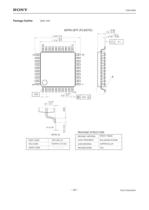
DETAIL A PACKAGE MATERIALLEAD TREATMENTLEAD MATERIALPACKAGE MASSEPOXY RESINPALLADIUM PLATINGCOPPER ALLOY SONY CODEEIAJ CODEJEDEC CODE 0.2gQFP-40P-L01P-QFP40-7x7-0.65
Open the catalog to page 20All Sony Semiconductors catalogs and technical brochures
 IMX901-AMR
2 Pages
 IMX490
2 Pages
 IMX290NQV
2 Pages
 ISX016
2 Pages
 IMX390CQV
2 Pages
Archived catalogs
 SLD344YT
6 Pages
 SLD432S
5 Pages
 CXA3314ER
16 Pages
 CXB1818Q
17 Pages
 ICX205AK
24 Pages
 CXA2096N
17 Pages
 SLD433S4
5 Pages
 CXA4416GC
21 Pages
 CXA2984GC SP4T ANT SW
11 Pages
 SLD335YT
5 Pages
 CXM3807K
24 Pages
 CXM3648UR
11 Pages
 CXM3645ER
12 Pages
 CXM3642K
29 Pages
 CXM3641ER
22 Pages
 CXM3632ER
22 Pages
 CXM3630UR
15 Pages
 CXM3617ER
23 Pages
 CXM3614ER
14 Pages
 CXM3604UR
14 Pages
 CXM3599UR
15 Pages
 CXM3593UR
11 Pages
 SLD1332V
5 Pages
 CXM3592AUR
15 Pages
 CXM3583AUR
17 Pages
 CXM3582UR
17 Pages
 CXM3580UR
13 Pages
 CXM3580AUR
17 Pages
 CXM3572ER
14 Pages
 CXM3570ER
13 Pages
 CXM3569XR
13 Pages
 ICX418ALB
20 Pages
 CXD4728R
68 Pages
 ICX642BKA
23 Pages
 CXA3791EN
13 Pages
 SLD332F
6 Pages
 CXG1407XR
11 Pages
 IMX291LQR
2 Pages
 IMX252LLR/LQR
2 Pages
 IMX230
2 Pages
 IMX377CQT
5 Pages
 IMX249LLJ/LQJ
2 Pages
 IMX323LQN
2 Pages
 IMX258
2 Pages
 IMX302LQJ
2 Pages
 CXD4017R
34 Pages
 CXA3197R
30 Pages
 IMX222LQJ
2 Pages
 IMX324
2 Pages
 IMX367LLA
2 Pages
 IMX412-AACK
2 Pages
 IMX385LQR
2 Pages
 IMX294CJK
2 Pages
 IMX253LLR/LQR
2 Pages
 IMX273LLR/LQR
2 Pages
 IMX183CLK-J/CQJ-J
2 Pages
 IMX249LLJ/IMX249LQJ
2 Pages
 IMX250LLR/LQR,IMX252LLR/LQR
2 Pages
 B/W Video Camera CCD ICX422AL
17 Pages
 B/W Video Camera CCD ICX279AL*2
18 Pages
 Color Video Camera CCD ICX239AKE
18 Pages
 Color Video Camera CCD ICX418AKL
22 Pages


- Liebherr display
- LCD display panel
- Color display panel
- LED display panel
- RGB display panel
- Compact display panel
- GNSS receiver
- Compact receiver
- Industrial receiver
- OLED display
- High-definition display module
- Satellite receiver
- Liebherr CMOS image sensor
- Vision sensor
- Communication card
- Full HD display
- Fiber laser diode
- Codec
- Liebherr visible image sensor