- Catalogs
- Sony Semiconductors
- Optical Communication Receiver IC CXA3668N
- Products
- Catalogs
- News & Trends
- Exhibitions
Optical Communication Receiver IC CXA3668N

Optical Communication Receiver IC CXA3668N
Catalog excerpts
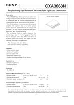
Description The CXA3668N is an IC that performs reception sideanalog signal processing for optical communication in combination with an infrared photodiode within aDigital Infrared Audio Transmission (DIAT) system.This IC incorporates a low noise trans-conductanceamplifier (I/V amplifier) that converts the opticalcurrent from the photodiode into a voltage andamplifies it, an AGC amplifier, a low-pass filter, band- pass filters, and an output amplifier.The band-pass filters are used to separate thedesired signal and the interfering signal. This chip has the two types of Full (3 to 6MHz) and Half (3 to4.5MHz) band-pass filters, and these can beswitched according to the application. 24 pin SSOP (Plastic) Full: Full-band width (3 to 6MHz) ? Half: Half-band width (3 to 4.5MHz) Features? Wide dynamic range ? On-chip I/V amplifier ? On-chip output filter ? Filter band switching pin ? Surface mounting package (24-pin SSOP) Applications? Infrared headphones ? Infrared speakers Structure Bi-CMOS IC Absolute Maximum Ratings (Ta = 25հC) ? Supply voltageV > CC I, V > CC 2, V > CC S, V > CC O3.3V ? Storage temperatureTstg55 to +150ְC ? Allowable power dissipationP > D 400mW Recommended Operating Conditions? Supply voltageV > CC I, V > CC 2, V > CC S, V > CC O2.3 to 2.7V ? Operating temperatureTopr40 to +85ְC 1 ֖ > E04244-PSSony reserves the right to change products and specifications without prior notice. This information does not convey any license byany implication or otherwise under any patents or other right. Application circuits shown, if any, are typical examples illustrating theoperation of the devices. Sony cannot assume responsibility for any problems arising out of the use of these circuits. size="-1">
Open the catalog to page 1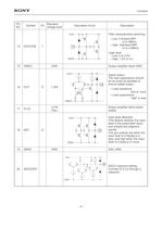
CXA3668N PinNo.SymbolStandardvoltage levelEquivalent circuitDescription14DIVCODE I/OFilter characteristics switching. > VccS GNDS ? Low: Full-band BPF(3 to 6MHz) I > 14 ? High: Half-band BPF(3 to 4.5MHz)Logic level: ? Low: 0 to 0.5V ? High: 1.5V to V > CC 15GNDOGNDOutput amplifier block GND. > VccO GNDO ? Load resistance:3k Ω or more > 16 ? Load capacitance:18pF or less17V 16OUT1.25V OSignal output.The load capacitance should be as small as possible to ensure stable output. > CC O+2.5V(Typ.)Output amplifier block powersupply. > Vcc2 GND2 18DET OInput level detection.This detects whether the input...
Open the catalog to page 4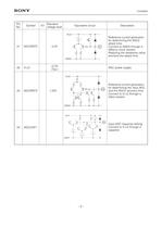
CXA3668N PinNo.SymbolStandardvoltage levelEquivalent circuitDescription21AGCIREF2 I/OReference current generationfor determining the AGC2 attack time. Connect to GND2 through a 390 Ω or more resistor.Reducing the resistance value shortens the attack time. > Vcc2 GND2 21 22V > CC 2+2.5V(Typ.)AGC power supply. > Vcc2 GND2 Reference current generationfor determining the input AGC and the AGC2 recovery time. Connect to V 23AGCIREF31.25V > 23 CC 2 through a33k Ω resistor. > Vcc2 GND2 24 Input AGC response setting.Connect to V 24AGCCAP1 > CC 2 through acapacitor. 0.2V 5 ֖ >
Open the catalog to page 5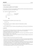
CXA3668N Description of Operation(1) Trans-impedance amplifier circuit (I/V amplifier) The input block is comprised of the trans-impedance amplifier circuit which converts the optical current Ip fromthe photodiode into a current, and the AGCATT circuit.Fig. 1 shows the I/V amplifier equivalent circuit. The following equations are satisfied in the circuit shown in Fig. 1.vo = A > Ztvovii Zt: Trans-impedanceA: Amplifier gain ֖A vivi ז vo = i Fig. 1 ZtThe input impedance Zi of the I/V amplifier is obtained from these equations as follows.Zi = vi/i = Zt/ (1 + A)The trans-impedance Zt of this IC is...
Open the catalog to page 8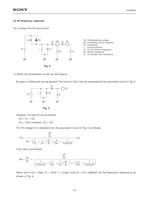
CXA3668N (3) IN frequency response Fig. 2 shows the IN input circuit. > Cd C2 C3INSISZsZiVdLPdVd: Photodiode bias voltageCd: Photodiode junction capacitor Pd: Photodiode L: External inductor C1, C2, C3: External capacitors Zs: SIS pin impedance Zi: I/V amplifier input impedance C1 Fig. 2 (1) When the photodiode current Ip ≤ 63.5Ap-pZs goes to 100k բĦ and can be ignored. The circuit in Fig. 2 can be expressed by the equivalent circuit in Fig. 3. > C5INZiLIp C4 Fig. 3 IpS > 2 C > 4 2 S > 3 + > When set to Cd = 72pF, C1 = 47pF, L = 6.8ɵH, and C2 = C3 = 6800pF, the Ga frequency response is asshown...
Open the catalog to page 9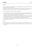
CXA3668N (6) AGC2 The band-pass filter output is amplified to 4 times by the preamplifier, and the GCA gain is varied so that thepreamplifier output is approximately 0.8Vp-p. The preamplifier output is converted from a differential signal to a single signal by a subtracter with a gain of approximately 2.1 times, and is then output from OUT (Pin 16) at a level of approximately 1.7Vp-p.? The AGC2 attack time and recovery time response are as follows.The attack time and the recovery time are determined by the capacitor Ca2 connected between AGCCAP2(Pin 20) and V > CC 2. Increasing the Ca2 value...
Open the catalog to page 12
CXA3668N Notes on Operation ? This IC has a high I/O gain (particularly during no signal or weak signal input of 0.15Ap-p (typ.) or less atwhich the AGC does not operate), so care should be taken for the power supply and GND pattern when designing the printed circuit board. The power supplies and GND are divided by function block as follows.1)Input blockPower supply: V Care should be taken for the following points when using the CXA3668N. > CC IGND: GNDI2)Input block shuntGND: GNDMOS3)AGC blockPower supply: V > CC 2GND: GND24)Filter blockPower supply: V > CC SGND: GNDS5)Output blockPower supply:...
Open the catalog to page 14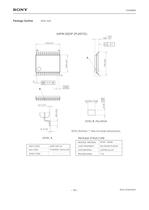
1.25 0.1+ 0.2 ֢ȗ 7.8 0.113 0.1 24 A > 7.6 ѱ 0.2 5.6 0.1 Ѣȗ b 0.13 M 0.65121 B b=0.22 0.03 > + 0.03 0.1 ѱ 0.1 > 0.15 0.01 0.5ֱ 0.2 DETAIL B : PALLADIUM 0˚ to 10˚ NOTE: Dimension " ∗ " does not include mold protrusion. DETAIL A > PACKAGE MATERIALLEAD TREATMENTLEAD MATERIALPACKAGE MASSEPOXY RESINPALLADIUM PLATINGCOPPER ALLOY SONY CODEEIAJ CODEJEDEC CODE SSOP-24P-L01P-SSOP24-7.8x5.6-0.65 0.1g
Open the catalog to page 16All Sony Semiconductors catalogs and technical brochures
 IMX901-AMR
2 Pages
 IMX490
2 Pages
 IMX290NQV
2 Pages
 ISX016
2 Pages
 IMX390CQV
2 Pages
Archived catalogs
 SLD344YT
6 Pages
 SLD432S
5 Pages
 CXA3314ER
16 Pages
 CXB1818Q
17 Pages
 ICX205AK
24 Pages
 CXA2096N
17 Pages
 SLD433S4
5 Pages
 CXA4416GC
21 Pages
 CXA2984GC SP4T ANT SW
11 Pages
 SLD335YT
5 Pages
 CXM3807K
24 Pages
 CXM3648UR
11 Pages
 CXM3645ER
12 Pages
 CXM3642K
29 Pages
 CXM3641ER
22 Pages
 CXM3632ER
22 Pages
 CXM3630UR
15 Pages
 CXM3617ER
23 Pages
 CXM3614ER
14 Pages
 CXM3604UR
14 Pages
 CXM3599UR
15 Pages
 CXM3593UR
11 Pages
 SLD1332V
5 Pages
 CXM3592AUR
15 Pages
 CXM3583AUR
17 Pages
 CXM3582UR
17 Pages
 CXM3580UR
13 Pages
 CXM3580AUR
17 Pages
 CXM3572ER
14 Pages
 CXM3570ER
13 Pages
 CXM3569XR
13 Pages
 ICX418ALB
20 Pages
 CXD4728R
68 Pages
 ICX642BKA
23 Pages
 CXA3791EN
13 Pages
 SLD332F
6 Pages
 CXG1407XR
11 Pages
 IMX291LQR
2 Pages
 IMX252LLR/LQR
2 Pages
 IMX230
2 Pages
 IMX377CQT
5 Pages
 IMX249LLJ/LQJ
2 Pages
 IMX323LQN
2 Pages
 IMX258
2 Pages
 IMX302LQJ
2 Pages
 CXD4017R
34 Pages
 CXA3197R
30 Pages
 IMX222LQJ
2 Pages
 IMX324
2 Pages
 IMX367LLA
2 Pages
 IMX412-AACK
2 Pages
 IMX385LQR
2 Pages
 IMX294CJK
2 Pages
 IMX253LLR/LQR
2 Pages
 IMX273LLR/LQR
2 Pages
 IMX183CLK-J/CQJ-J
2 Pages
 IMX249LLJ/IMX249LQJ
2 Pages
 IMX250LLR/LQR,IMX252LLR/LQR
2 Pages
 B/W Video Camera CCD ICX422AL
17 Pages
 B/W Video Camera CCD ICX279AL*2
18 Pages
 Color Video Camera CCD ICX239AKE
18 Pages
 Color Video Camera CCD ICX418AKL
22 Pages


- Liebherr display
- LCD display panel
- Color display panel
- LED display panel
- RGB display panel
- Compact display panel
- GNSS receiver
- Compact receiver
- Industrial receiver
- OLED display
- High-definition display module
- Laser diode
- Satellite receiver
- Liebherr CMOS image sensor
- Vision sensor
- Communication card
- Full HD display
- Fiber laser diode
- Codec
- Liebherr visible image sensor