
- Catalogs
- Sony Semiconductors
- Networking High-Speed Synchronous SRAMs CXK79M72C164GB

- Products
- Catalogs
- News & Trends
- Exhibitions
Networking High-Speed Synchronous SRAMs CXK79M72C164GB

1 / 28 PagesView full catalog
Networking High-Speed Synchronous SRAMs CXK79M72C164GB
Product catalog summary
Overview: This document provides detailed technical specifications and operational features of Sony's high-speed synchronous SRAMs, specifically the CXK79M72C164GB and CXK79M36C164GB models. These SRAMs are designed for high-performance applications and feature CMOS static RAMs with common I/O pins.
Specifications:
- Memory Organization: CXK79M72C164GB is organized as 262,144 words by 72 bits, and CXK79M36C164GB as 524,288 words by 36 bits.
- Package: JEDEC-standard 209 pin BGA package.
- Operation: Supports Single Data Rate (SDR) Pipelined read operations and Double Late Write (DLW) write operations.
- Clock: Positive and negative output clocks for source-synchronous operation.
- Speed: Operates at 350 MHz with a single 1.8V power supply.
- JTAG: Boundary scan interface using IEEE standard 1149.1 protocol.
Features:
- Speed Bins: Options include cycle times of 2.85ns, 3.0ns, 3.3ns, and 4.0ns.
- Power Supply: Single 1.8V core power supply with VDDQ ranging from 1.4V to VDD.
- I/O Interface: HSTL-compatible with a dedicated input reference voltage (VREF).
- Burst Capability: Internally controlled Linear Burst address sequencing with lengths of two, three, or four.
- Output Driver Impedance: Programmable via the ZQ control pin.
- Depth Expansion: Supported via programmable chip enables.
Operational Details:
- Clock Truth Table: Describes logic states for various operations.
- State Diagram: Illustrates transitions between operational states.
- Burst Operations: Describes sequence and address wrapping.
- Depth Expansion: Use of programmable chip enables.
- Output Driver Impedance Control: Method for setting impedance using an external resistor.
- Power-Up Sequence: Recommended sequence for reliability.
Absolute Maximum Ratings: Lists maximum stress ratings for supply voltage, input voltage, operating temperature, and storage temperature.
Thermal Characteristics: Provides junction to case temperature rating.
I/O Capacitance: Details input and output capacitance under specified test conditions.
Electrical Characteristics:
- Supply Voltage: VDD ranges from 1.7V to 1.95V, VDDQ from 1.4V to VDD.
- Input Reference Voltage: VREF is VDDQ/2 with a tolerance of ±0.1V.
Procedures:
- Guidelines for connecting the CK input clock to VREF.
- Conditions for differential input clocks.
Norms and Standards: Adheres to IEEE std. 1149.1 for JTAG Test Access Port and Boundary Scan interface.
Recommendations: For maximum output drive, tie the ZQ pin to VSS; for minimum, leave unconnected or tie to VDDQ.
AC and DC Electrical Characteristics: Includes input and output leakage currents, power supply operating current, and output driver impedance.
Test Conditions: AC test conditions specified for VDDQ at 1.8V and 1.5V.
JTAG Test Mode: Describes TAP controller operations, TAP registers, and timing diagrams.
Figures and Diagrams: Includes timing diagrams for read-write-read operations and TAP controller state diagram.
Ordering Information:
- Part numbers include CXK79M72C164GB and CXK79M36C164GB.
- Speed options range from 2.85ns to 4.0ns cycle times.
Package Details:
- 209 Pin BGA package with epoxy resin and copper-clad laminate materials.
- Package mass is 1.1g.
Revision History: Includes modifications to electrical characteristics, pin assignments, and new speed bins.
Key Notes:
- Some instructions and register codes are reserved for manufacturer use only.
- Boundary Scan Register bit order assignments detailed for both x72 and x36 configurations.
See more
Catalog excerpts
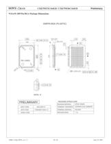
PACKAGE MATERIALTERMINAL TREATMENTTERMINAL MATERIALPACKAGE MASSEPOXY RESINCOPPER-CLAD LAMINATESOLDER1.1g SONY CODEJEITA CODEJEDEC CODEBGA-209P-01P-BGA209-14X22-1.0
Open the catalog to page 26All Sony Semiconductors catalogs and technical brochures
 IMX901-AMR
2 Pages
 IMX490
2 Pages
 IMX290NQV
2 Pages
 ISX016
2 Pages
 IMX390CQV
2 Pages
Archived catalogs
 SLD344YT
6 Pages
 SLD432S
5 Pages
 CXA3314ER
16 Pages
 CXB1818Q
17 Pages
 ICX205AK
24 Pages
 CXA2096N
17 Pages
 SLD433S4
5 Pages
 CXA4416GC
21 Pages
 CXA2984GC SP4T ANT SW
11 Pages
 SLD335YT
5 Pages
 CXM3807K
24 Pages
 CXM3648UR
11 Pages
 CXM3645ER
12 Pages
 CXM3642K
29 Pages
 CXM3641ER
22 Pages
 CXM3632ER
22 Pages
 CXM3630UR
15 Pages
 CXM3617ER
23 Pages
 CXM3614ER
14 Pages
 CXM3604UR
14 Pages
 CXM3599UR
15 Pages
 CXM3593UR
11 Pages
 SLD1332V
5 Pages
 CXM3592AUR
15 Pages
 CXM3583AUR
17 Pages
 CXM3582UR
17 Pages
 CXM3580UR
13 Pages
 CXM3580AUR
17 Pages
 CXM3572ER
14 Pages
 CXM3570ER
13 Pages
 CXM3569XR
13 Pages
 ICX418ALB
20 Pages
 CXD4728R
68 Pages
 ICX642BKA
23 Pages
 CXA3791EN
13 Pages
 SLD332F
6 Pages
 CXG1407XR
11 Pages
 IMX291LQR
2 Pages
 IMX252LLR/LQR
2 Pages
 IMX230
2 Pages
 IMX377CQT
5 Pages
 IMX249LLJ/LQJ
2 Pages
 IMX323LQN
2 Pages
 IMX258
2 Pages
 IMX302LQJ
2 Pages
 CXD4017R
34 Pages
 CXA3197R
30 Pages
 IMX222LQJ
2 Pages
 IMX324
2 Pages
 IMX367LLA
2 Pages
 IMX412-AACK
2 Pages
 IMX385LQR
2 Pages
 IMX294CJK
2 Pages
 IMX253LLR/LQR
2 Pages
 IMX273LLR/LQR
2 Pages
 IMX183CLK-J/CQJ-J
2 Pages
 IMX249LLJ/IMX249LQJ
2 Pages
 IMX250LLR/LQR,IMX252LLR/LQR
2 Pages
 B/W Video Camera CCD ICX422AL
17 Pages
 B/W Video Camera CCD ICX279AL*2
18 Pages
 Color Video Camera CCD ICX239AKE
18 Pages
 Color Video Camera CCD ICX418AKL
22 Pages


Related Searches
- Display module
- LCD display panel
- Color display panel
- LED display panel
- RGB display panel
- Compact display panel
- GNSS receiver
- Compact receiver
- Industrial receiver
- OLED display
- High-definition display module
- Laser diode
- Satellite receiver
- Sony CMOS image sensor
- Vision sensor
- Communication card
- Full HD display
- Fiber laser diode
- Sony visible image sensor
- Sony infrared image sensor
*Prices are pre-tax. They exclude delivery charges and customs duties and do not include additional charges for installation or activation options. Prices are indicative only and may vary by country, with changes to the cost of raw materials and exchange rates.
About DirectIndustry
DirectIndustry is a marketplace that offers B2B players a complete experience, from product sourcing to purchase. DirectIndustry is an entity of VirtualExpo Group.
Are you a buyer?
Are you a supplier?