- Catalogs
- Sony Semiconductors
- Mixed Signal Systems D/A Converter Lineup CXD1171M
- Products
- Catalogs
- News & Trends
- Exhibitions
Mixed Signal Systems D/A Converter Lineup CXD1171M

Mixed Signal Systems D/A Converter Lineup CXD1171M
The CXD1171M is an 8-bit, 40 MHz high-speed D/A converter designed for digital TV and graphic display applications. It features a resolution of 8 bits, a maximum conversion speed of 40 MSPS, and low power consumption of 80 mW with a 200 Ω load at 2 Vp-p output. The device operates with a single +5 V power supply and is TTL CMOS compatible.
Absolute Maximum Ratings:
- Supply voltage (AVDD, DVDD): 7 V
- Input voltage: VDD +0.5 to VSS –0.5 V
- Output current: 15 mA
- Storage temperature: –55 to +150 °C
Recommended Operating Conditions:
- Supply voltage: 4.75 to 5.25 V
- Reference input voltage: 2.0 V
- Clock pulse width: 11.2 ns (min) to 1.1 µs (max)
- Operating temperature: –40 to +85 °C
Features:
- Non-linearity error within ±0.25 LSB
- Low glitch noise
- Silicon gate CMOS IC structure
Block Diagram and Pin Configuration:
The document provides a detailed block diagram and pin configuration for the CXD1171M, highlighting the current cells, latches, decoder, clock generator, and bias voltage generator.
Electrical Characteristics:
The electrical characteristics are measured under specific conditions (FCLK=40 MHz, AVDD=DVDD=5 V, ROUT=200 Ω, VREF=2.0 V, Ta=25 °C) and include parameters such as resolution, conversion speed, integral and differential non-linearity errors, output full-scale voltage and current, glitch energy, and supply current.
Operation Notes:
- Output resistance selection: The output resistance should be calculated based on the relation VFS = IFS × ROUT, with considerations for power consumption and glitch energy.
- Phase relation: Proper phase relation between data and clock is necessary to achieve expected performance.
- Power supply and ground: Separate analog and digital systems to reduce noise effects.
- Latch up prevention: Ensure common power supply sources for AVDD and DVDD to prevent latch up.
Application Circuit:
The document includes a typical application circuit for the CXD1171M, illustrating the connections for digital input, power supply, and output.
Package Outline:
The CXD1171M is housed in a 24-pin SOP plastic package with specific dimensions and lead specifications.
Catalog excerpts
Description The CXD1171M is a 8-bit 40 MHz high speed D/Aconverter. The adoption of a current output system reduces power consumption to 80 mW (200 Ω loadat 2 Vp-p output).This IC is suitable for digital TV and graphicdisplay applications. 24 pin SOP (Plastic) Features? Resolution 8-bit ? Max. conversion speed 40MSPS ? Non linearity error within 0.25 LSB Absolute Maximum Ratings (Ta=25 ѰC) ? Low glitch noise Supply voltageAV > DD , DV > DD 7V ? TTL CMOS compatible input ? Input voltage (All pins)V ? +5 V single power supply > IN V > DD +0.5 to V > SS Ֆ0.5V ? Low power consumption 80 mW(200 ? Output currentI > OUT 15mA Ω load at 2 Vp-p output) ? Storage temperatureTstg55 to +150ְC Function 8-bit 40 MHz D/A converter Recommended Operating Conditions? Supply voltageAV > DD , AV > SS 4.75 to 5.25VDV Structure > DD , DV > SS 4.75 to 5.25V Silicon gate CMOS IC ? Reference input voltageV > REF 2.0V ? Clock pulse widthTpw > 1 ,Tpw > 11.2 ns (min) to 1.1 s (max) ? Operating temperatureToprՖ40 to +85C > Sony reserves the right to change products and specifications without prior notice. This information does not convey any license byany implication or otherwise under any patents or other right. Application circuits shown, if any, are typical examples illustrating theoperation of the devices. Sony cannot assume responsibility for any problems arising out of the use of these circuits. З1 > E89X38G13-PS size="-1">
Open the catalog to page 1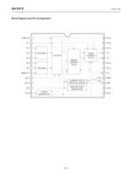
(LSB) D0 D1 D2 D3 D4 D5 D6(MSB) D7BLK DV 1 24 > DD 2 23 DV > DD 3 22 AV > DD 4 DECODER 2LSB'SCURRENTCELLS 21 IO IOAV LATCHES 5 20 6MSB'SCURRENTCELLS 6 19 > DD 7 DECODER 18 AV > DD 8 17 VGVREFIREFAV 9 16 CURRENT CELLS(FOR FULL SCALE) > SS 10 15 VB CLK DV 11 BIAS VOLTAGEGENERATOR 14 > SS 12 CLOCKGENERATOR 13 DV > SS
Open the catalog to page 2
CXD1171M Notes on Operation? How to select the output resistanceThe CXD1171M is a D/A converter of the current output type. To obtain the output voltage connect the resistance to the current output pin IO. For specifications we have:Output full scale voltageV > FS = 1.9 to 2.1 [V]Output full scale currentI > FS = less than 15 [mA]Calculate the output resistance value from the relation of V > FS = I > FS R > OUT . Also, 16 times resistance of theoutput resistance is connected to reference current pin IREF. In some cases, however, this turns out to be a value that does not actually exist. In such...
Open the catalog to page 8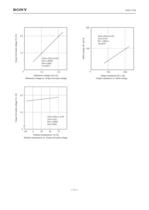
CXD1171M > [V] AV > DD =DV > DD =5.0VV > FS REF =2.0VR > IR 16R ≈ > OUT Ta=25CAV > DD =DV > DD =5.0VR > Glitch energy GE [pVзs] Output full scale voltage V OUT =200 Ω R > IR =3.3k Ω Ta=25C0 1.001.02.0 Reference voltage vs. Output full scale voltageReference voltage V 2.0 100 100 Output resistance vs. Glitch energyOutput resistance R 200 200 > REF [V] > OUT [ ТĦ ] > [V] FS 1.92.0 Ambient temperature vs. Output full scale voltageAmbient temperature Ta [C] AV > DD =DV > DD = 5.0VV > REF =2.0VR > Output full-scale voltage V OUT =200 ТĦ R > IR =3.3k Ω 0255075250 >
Open the catalog to page 11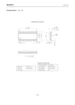
MOLDING COMPOUNDLEAD TREATMENTLEAD MATERIALPACKAGE MASSEPOXY RESINSOLDER PLATING42/COPPER ALLOY SONY CODEEIAJ CODEJEDEC CODE SOP-24P-L01SOP024-P-0300 0.3g
Open the catalog to page 12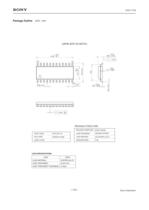
MOLDING COMPOUNDLEAD TREATMENTLEAD MATERIALPACKAGE MASSEPOXY RESINSOLDER PLATING42/COPPER ALLOY SONY CODEEIAJ CODEJEDEC CODE SOP-24P-L01SOP024-P-0300 0.3g LEAD SPECIFICATIONS ITEMLEAD MATERIALCOPPER ALLOYLEAD TREATMENTSn-Bi 2.5%LEAD TREATMENT THICKNESS5-18 mSPEC. >
Open the catalog to page 13All Sony Semiconductors catalogs and technical brochures
 IMX901-AMR
2 Pages
 IMX490
2 Pages
 IMX290NQV
2 Pages
 ISX016
2 Pages
 IMX390CQV
2 Pages
Archived catalogs
 SLD344YT
6 Pages
 SLD432S
5 Pages
 CXA3314ER
16 Pages
 CXB1818Q
17 Pages
 ICX205AK
24 Pages
 CXA2096N
17 Pages
 SLD433S4
5 Pages
 CXA4416GC
21 Pages
 CXA2984GC SP4T ANT SW
11 Pages
 SLD335YT
5 Pages
 CXM3807K
24 Pages
 CXM3648UR
11 Pages
 CXM3645ER
12 Pages
 CXM3642K
29 Pages
 CXM3641ER
22 Pages
 CXM3632ER
22 Pages
 CXM3630UR
15 Pages
 CXM3617ER
23 Pages
 CXM3614ER
14 Pages
 CXM3604UR
14 Pages
 CXM3599UR
15 Pages
 CXM3593UR
11 Pages
 SLD1332V
5 Pages
 CXM3592AUR
15 Pages
 CXM3583AUR
17 Pages
 CXM3582UR
17 Pages
 CXM3580UR
13 Pages
 CXM3580AUR
17 Pages
 CXM3572ER
14 Pages
 CXM3570ER
13 Pages
 CXM3569XR
13 Pages
 ICX418ALB
20 Pages
 CXD4728R
68 Pages
 ICX642BKA
23 Pages
 CXA3791EN
13 Pages
 SLD332F
6 Pages
 CXG1407XR
11 Pages
 IMX291LQR
2 Pages
 IMX252LLR/LQR
2 Pages
 IMX230
2 Pages
 IMX377CQT
5 Pages
 IMX249LLJ/LQJ
2 Pages
 IMX323LQN
2 Pages
 IMX258
2 Pages
 IMX302LQJ
2 Pages
 CXD4017R
34 Pages
 CXA3197R
30 Pages
 IMX222LQJ
2 Pages
 IMX324
2 Pages
 IMX367LLA
2 Pages
 IMX412-AACK
2 Pages
 IMX385LQR
2 Pages
 IMX294CJK
2 Pages
 IMX253LLR/LQR
2 Pages
 IMX273LLR/LQR
2 Pages
 IMX183CLK-J/CQJ-J
2 Pages
 IMX249LLJ/IMX249LQJ
2 Pages
 IMX250LLR/LQR,IMX252LLR/LQR
2 Pages
 B/W Video Camera CCD ICX422AL
17 Pages
 B/W Video Camera CCD ICX279AL*2
18 Pages
 Color Video Camera CCD ICX239AKE
18 Pages
 Color Video Camera CCD ICX418AKL
22 Pages


- LCD display panel
- Color display panel
- LED display panel
- RGB display panel
- Compact display panel
- GNSS receiver
- Compact receiver
- Industrial receiver
- OLED display
- High-definition display module
- Laser diode
- Satellite receiver
- Liebherr CMOS image sensor
- Vision sensor
- Communication card
- Full HD display
- Fiber laser diode
- Codec
- Liebherr visible image sensor