- Catalogs
- Sony Semiconductors
- Mixed Signal Systems A/D Converter Lineup CXA3256R
- Products
- Catalogs
- News & Trends
- Exhibitions
Mixed Signal Systems A/D Converter Lineup CXA3256R

Mixed Signal Systems A/D Converter Lineup CXA3256R
- Differential and integral linearity error: ±0.5LSB or less
- High-speed operation up to 120MSPS
- Low input capacitance of 10pF
- Wide analog input bandwidth of 250MHz
- Low power consumption at 500mW
- Power saving function and 1:2 demultiplexed output
- Compatible with ECL, PECL, and TTL digital input levels
- Single +5V power supply operation
- Ultra-small 48-pin LQFP package
- Supply voltage: +4.75 to +5.25V
- Analog input voltage: VRB to VRT
- Reference input voltage: VRT 2.9 to 4.1V, VRB 1.4 to 2.6V
- Maximum conversion rate: 120MSPS in DMUX mode
- Operating temperature: -20 to +75°C
Catalog excerpts
CXA3256R Pin Description and I/O Pin Equivalent Circuit PinNo.SymbolI/O Standardvoltage level Equivalent circuitDescription 3, 105, 820, 2932, 4119, 3031, 4212 1 AGNDAV Analog ground.Separated from the digital ground.Analog power supply.Separated from the digital power supply.Digital ground.Digital power supply.Digital power supply.Ground for ECL input. +5V for PECL and TTL inputs. Digital power supply.5V for ECL input. Ground for PECL and TTL inputs.Data output switching.Data is output from both the PA side and PB side by setting this pin open. When set to DVcc1 level, only the PA side output...
Open the catalog to page 5
EE OSC1 φ : Variable AV > CC 4V1.95V2V 5V5VIccI V > RT DV > CC 1DV > IN 8fr1024samples > CC 2PSDGND3DGND2DGND1 AGNDCLK/EDV CXA3256R LogicAnalizer V > IN 5MHz PECL OSC2 V > RB EE 3 100MHz 100MHzAmp ECLBufferCLKV > +V VS2S1S1: ON when A < BS2: ON when A > B V > RT V > IN V > RM 2V > RB CLKV ֢Ȇυ∆ 129128 127126125Sampling timing fluctuation(= aperture jitter) t A < B A > BComparatorA8toA1A0B8toB1B0 > IN σ (LSB) > IN 8 8 CXA3256R Buffer CLK 1Ӕ0Ӕ00000to11110V DVM Where σ (LSB) is the deviation of the output codes whenthe largest slew rate point is sampled at the clock which has exactly the same...
Open the catalog to page 11
Tds N 2 1.4ns (typ.) > IN N֖ 1 N + 3N + 1N + 4N +5 T NN + 6 CLKV Tpw1N + 2 Tpw0 3.5ns (min)7.5ns (max) 7.0ns (max) 2.0V0.8V N + 2 PBD0 to D7PAD0 to D7N 2.0V0.8VTdo1 N + 1 N + 3 Td_clk; 4.5ns (typ.) T + 0.5ns (typ.) ≈ T ≈ T 3.0ns (min) (Pin 6)(Pin 13) (Pins 21 to 28)(Pins 33 to 40) (Pin 43)(Pin 48) CLK OUTRESETN 2.0V 2.0V (Reset period) 0.8V Tdo2; 5.0ns (typ.) 0.8V 2.0V 0.8V T_rh T_rs T_rh T_rs >
Open the catalog to page 17
CXA3256R Notes on Operation? The CXA3256R has the PECL and TTL input pins for the clock and reset input pins. When the clock is inputin PECL level, inputting the reset signal in PECL level is recommended. Also, when the clock is input in TTL level, inputting the reset signal in TTL is recommended. ? The impedance of the input signal should be properly matched to ensure the CXA3256R's stable operation atthe high speed. ? In the CXA3256R, all the TTL input pins become the high level when left open. ? The power supply and grounding have a profound influence on converter performance. The power supplyand...
Open the catalog to page 19
CXA3256R ? When the digital input level is ECL or PECL level, ∗∗∗ /E pins should be used and ∗∗∗ /T pins left open. Whenthe digital input level is TTL, ∗∗∗ /T pins should be used and ∗∗∗ /E pins left open. ? ? The CXA3256R TTL output high level is clamped to approximately 2.8 V in the IC.This makes it possible todirectly interface with the 3.3V system CMOS IC. However,the CXA3256R has the VOCLP pin which is used to clamp the TTL output high level. See the Example of Representative Characteristics for the relationship between the VOCLP pin and the TTL high level. The CXA3026Q has the output pins...
Open the catalog to page 20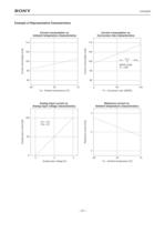
fin = 1kHz f > CLK 4 DMUX modeC > L = 5pF 95100 105110 95100 105110 120 > Current consumption [mA] Current consumption [mA] Ta֖ Ambient temperature [C]Ж25902575 Fc Conversion rate [MSPS]09060 > RT = 4VV > RB = 2V 34V 50100 0 > Reference current [mA] Analog input current [ֵA] Analog input voltage [V]234 Ta Ambient temperature [ְC]2522575 >
Open the catalog to page 21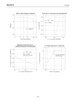
6 CLK 10 > ֖7 4 Error > 16LSBfin = 1kHzf 10 > ֖8 SNR [dB] 304050 30310 Fc = 120MSPS > Error Rate [TPS] 10 > 9 10 > ֖10 120140160 10 Input frequency [MHz]120550 Fc Conversion rate [MSPS] > fin =֖ 1kHz f > CLK 4 Error > 16LSB Error rate: 10 > 9 TPS TTL high level whenVOCLP is open. 150170 23 140 160 > TTL output high level [V] Fc֖ Maximum conversion rate [MSPS] 1 Ta Ambient temperature [ְC]251302575 VOCLP pin voltage [V]0.5135 >
Open the catalog to page 22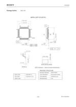
PACKAGE MATERIALLEAD TREATMENTLEAD MATERIALPACKAGE MASSEPOXY RESINCOPPER ALLOY SONY CODEEIAJ CODEJEDEC CODE PALLADIUM PLATING 0.2gLQFP-48P-L01P-LQFP48-7x7-0.5
Open the catalog to page 23All Sony Semiconductors catalogs and technical brochures
 IMX901-AMR
2 Pages
 IMX490
2 Pages
 IMX290NQV
2 Pages
 ISX016
2 Pages
 IMX390CQV
2 Pages
Archived catalogs
 SLD344YT
6 Pages
 SLD432S
5 Pages
 CXA3314ER
16 Pages
 CXB1818Q
17 Pages
 ICX205AK
24 Pages
 CXA2096N
17 Pages
 SLD433S4
5 Pages
 CXA4416GC
21 Pages
 CXA2984GC SP4T ANT SW
11 Pages
 SLD335YT
5 Pages
 CXM3807K
24 Pages
 CXM3648UR
11 Pages
 CXM3645ER
12 Pages
 CXM3642K
29 Pages
 CXM3641ER
22 Pages
 CXM3632ER
22 Pages
 CXM3630UR
15 Pages
 CXM3617ER
23 Pages
 CXM3614ER
14 Pages
 CXM3604UR
14 Pages
 CXM3599UR
15 Pages
 CXM3593UR
11 Pages
 SLD1332V
5 Pages
 CXM3592AUR
15 Pages
 CXM3583AUR
17 Pages
 CXM3582UR
17 Pages
 CXM3580UR
13 Pages
 CXM3580AUR
17 Pages
 CXM3572ER
14 Pages
 CXM3570ER
13 Pages
 CXM3569XR
13 Pages
 ICX418ALB
20 Pages
 CXD4728R
68 Pages
 ICX642BKA
23 Pages
 CXA3791EN
13 Pages
 SLD332F
6 Pages
 CXG1407XR
11 Pages
 IMX291LQR
2 Pages
 IMX252LLR/LQR
2 Pages
 IMX230
2 Pages
 IMX377CQT
5 Pages
 IMX249LLJ/LQJ
2 Pages
 IMX323LQN
2 Pages
 IMX258
2 Pages
 IMX302LQJ
2 Pages
 CXD4017R
34 Pages
 CXA3197R
30 Pages
 IMX222LQJ
2 Pages
 IMX324
2 Pages
 IMX367LLA
2 Pages
 IMX412-AACK
2 Pages
 IMX385LQR
2 Pages
 IMX294CJK
2 Pages
 IMX253LLR/LQR
2 Pages
 IMX273LLR/LQR
2 Pages
 IMX183CLK-J/CQJ-J
2 Pages
 IMX249LLJ/IMX249LQJ
2 Pages
 IMX250LLR/LQR,IMX252LLR/LQR
2 Pages
 B/W Video Camera CCD ICX422AL
17 Pages
 B/W Video Camera CCD ICX279AL*2
18 Pages
 Color Video Camera CCD ICX239AKE
18 Pages
 Color Video Camera CCD ICX418AKL
22 Pages


- Liebherr display
- LCD display panel
- Color display panel
- LED display panel
- RGB display panel
- Compact display panel
- GNSS receiver
- Compact receiver
- Industrial receiver
- OLED display
- High-definition display module
- Laser diode
- Satellite receiver
- Liebherr CMOS image sensor
- Vision sensor
- Communication card
- Full HD display
- Fiber laser diode
- Codec
- Liebherr visible image sensor