
- Catalogs
- Sony Semiconductors
- Mixed Signal Systems D/A Converter Lineup CXA3197R

- Products
- Catalogs
- News & Trends
- Exhibitions
Mixed Signal Systems D/A Converter Lineup CXA3197R

Mixed Signal Systems D/A Converter Lineup CXA3197R
- Maximum Conversion Rate: 125MSPS (PECL), 100MSPS (TTL)
- Resolution: 10 bits
- Power Consumption: 480mW (typical)
- Data Input Level: TTL
- Clock and Reset Input Level: TTL and PECL compatible
- Voltage Output: Capable of driving a 50Ω load
- 2:1 Multiplexed Input Function
- 1/2 Frequency-Divided Clock Output via Built-in Divider Circuit
- Reset Signal Polarity Switching Function
- Supply Voltage: -0.5V to +6.0V
- Input Voltage: Varies by pin type (Analog, Digital, PECL)
- Storage Temperature: -65°C to +150°C
- Power Dissipation: 1.4W
- MUX.1A Mode: Halves the clock frequency internally and outputs a 1/2 frequency-divided signal at TTL level. Data is synchronized with this signal for analog output.
- MUX.1B Mode: Similar to MUX.1A but the 1/2 frequency-divided signal is not observable. Data is loaded based on clock and reset signals.
- MUX.2 Mode: Uses a DIV2IN signal synchronized with the clock for data loading, allowing for internal multiplexing and analog output.
- SELE.A and SELE.B Modes: Allow selection between two data input systems (A and B) for analog output, with switching controlled by the C2 pin.
Catalog excerpts
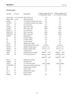
CXA3197R Pin Description [Symbol][Pin No.][Description] DA0 to DA91 to 6, 45 to 48Side A data input.TTLTTLDB0 to DB97 to 16Side B data input.TTLTTL DIV2IN171/2 frequency-divided clock input.TTLTTL DIV2OUT181/2 frequency-divided clock output.TTLTTL CLK/T19TTL clock input.TTLTTL CLKP/E20PECL clock input.PECLPECL CLKN/E21PECL clock input.PECLPECL RESET/T22TTL reset input.TTLTTL RESETP/E23PECL reset input.PECLPECL RESETN/E24PECL reset input.PECLPECL DGND225Digital ground.0V5V C126Function setting.TTLTTL C227Function setting.TTLTTL C328Function setting.TTLTTL DV > Typical voltage level for Typical...
Open the catalog to page 3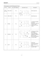
CXA3197R Pin Description and I/O Pin Equivalent Circuit Pin No.Symbol Typical voltage level Equivalent circuitDescriptionI/O > DV CC 1 DGND1 Side A data input. > 1 6 45 48 7 16tototo1.5V Side B data input. > DV CC 1 DGND1 1/2 frequency-divided clock input. Use this pin in MUX.1A or MUX.2 mode. Leave open for other modes.1/2 frequency-divided clock output. The 1/2 frequency- divided clock signal (DIV2OUT) is output in MUX.1A mode. Set to high impedance for other modes. DA0 to DA9DB0 to DB9 DIV2IN DIV2OUT TTLTTL TTL TTL 1 to 645 to 487 to 16 17 18 II I O > 171.5V DV CC 1 DGND1 18 100K DV CC 1 DGND1...
Open the catalog to page 5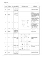
CXA3197R Pin No.Symbol Typical voltage level Equivalent circuitDescriptionI/O AV DV > CC 229 Digital power supply.Analog output power supply. The AV Ω , the inverse output pin should also be terminated with 50 Ω even if the inverse output is not used. AV > CC O pin voltage can be varied within the range that satisfies the analog output compliance voltage. Positive analog output.Analog ground. Negative analog output.The inverse of the positive analog output pin is output. When the positive output is terminated with 50 > CC OSingle power supply: +5V Dual power supply: GND30 AOUTNAV > AV CC O AGND2...
Open the catalog to page 7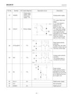
CXA3197R Pin No.Symbol Typical voltage level Equivalent circuitDescriptionI/OAnalog power supply.AGND2Single power supply: GND Dual power supply:5V37 TTL output High level clamp. A TTL level signal is output from the DIV2OUT pin in MUX.1A mode. The TTL High level voltage can be clamped to the value approximately equivalent to the voltage applied to this pin. Leave the VOCLP pin open for other modes.VOCLPClamp voltage38I > DV CC 1 DGND1 38 DV CC 1 DGND1 Reset signal polarity switching. At High level, the reset polarity is active Low; at Low level, active High. R POLARITY TTL39I > 391.5V DV CC...
Open the catalog to page 8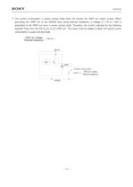
REFOUT AV > CC 2 AGND2In power saving mode:I BGR 34VREF > REFOUT = VREF pin voltageExternal resistance >
Open the catalog to page 11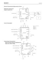
CC 1DGND1DV > CC 2AV > CC 2AV 10DA0 to DA9 > CC OAOUTPAOUTNVSETDGND2AGND2 10-bit Data input +5VDV 50 Ω 10DB0 to DB9CLK/T 50 Ω 1MHz TTL CLKCXA3197R 937.5mV5V֖5V+5V DVM(Digital Voltmeter) C1C2C3 PC +5V I > 1 I > 2 I > 3 I > 4 CC = I > 1 + I > 2 + I > 3 + I > 4 DI > CC 1 = I > 1 DV > CC 1DV > CC 2AV > CC 2AV > CC O DI > CC 2 = I > 2 AI > CC 2 = I > 3 10DA0 to DA9 AI > CC O = I > 4 AOUTPAOUTNVSETDGND1DGND2 AGND2C1C2C3 Low for all side B data 10DB0 to DB9DIV2INHigh for all side A data1MHz TTL CLK +5CLK/TDIV2OUTPSCXA3197R I 937.5mV > CC 1DGND1DV > CC 2AV High for all side A dataLow for all side B data...
Open the catalog to page 14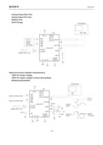
+5VDV 50 Ω 50 Ω > CC 1DGND1DV > CC 2AV D. P. G.(Digital Pattern Generator) 10DA0 to DA9 > CC 2AV AOUTPAOUTNVREFDGND2AGND2C1C2C3CLKP/E > CC O 10DB0 to DB9100MHz PECL CLK CLKN/ECXA3197R VSET 5V +5V ֖5V Oscilloscope Oscilloscope +5VDV > CC 1DGND1DV > CC 2AV 50 Ω 10DA0 to DA9 > CC 2AV > CC O AOUTPAOUTNVREFDGND2AGND2C1C2C3CLKP/E > CC O(= 0V) AGND2+ 937.5mV 10DB0 to DB920MHz PECL CLK V > FS Ω AOUTPoutput CLKN/ECXA3197R 1mA 0.1F High for all side A dataHigh for all side B data +5VPS 50 բĦ VSET pin output AV 100mVp-p 5VVSET +5V ֖5V 50 >
Open the catalog to page 15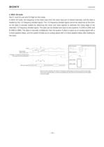
CXA3197R (MUX.1B mode) Clock 1/2 th-rst ts-rst Reset signal(when active Low)Internally 1/2 frequency-divided signal(This signal cannot be observed.)Data input signal Reset input pin tsth DB0 to DB9 After the reset is released, the internal 1/2 frequency-divided signal commences at the first clock edge, so be sure to input the data in a manner that satisfies the setup time (ts) and hold time (th) with respect to this clock edge. Clock input pin DA0 to DA9 >
Open the catalog to page 19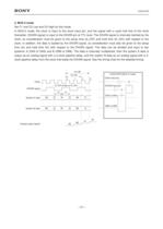
PD (B)0123 t > PD (A)t CXA3197R (MUX.2 mode) Clock input pinDIV2IN input pin ts_DIVth_DIV ts th DA0 to DA9 A1 A2B0 DB0 to DB9 B1 B2 ClockDIV2IN signalSystem A dataSystem B dataAnalog output signalB1 A0B0A1 A0 >
Open the catalog to page 21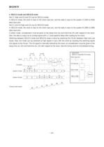
t > PD (A)t > PD (B)0101 ts_C2 th_C2 thts DA0 to DA9 CXA3197R(SELE.A mode/SELE.B mode) A0 A1 A2 A6ClockC2 signalSystem A dataSystem B dataAnalog output signal A8 Select DB0 to DB9 Clock input pinC2 input pin B3 B4 B5 B7 B3B4B5A6 A0A1A2 >
Open the catalog to page 22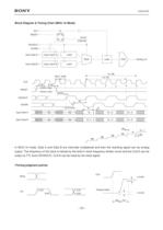
R CLK/2(Internal)Analog outInput Data AInput Data BDIV2INDIV2OUTRESETCLK DQQ Input Latch A Latch MUX Latch DAC Input Latch B Latch t > PD (B) Tpw1Tpw0 t > PD (A) CLKRESETDIV2OUTInput Data AInput Data BDIV2IN N$N$N$N$NN + 1 ts-rst th-rsttd-DIV0123 4 5 2T-tm (Active High) (Active Low) tm ts th N$ N$N + 2N + 4N N$ N$N + 3N + 5N +1 tdo tdo >
Open the catalog to page 23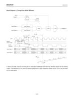
R CLK/2(Internal)Analog outInput Data AInput Data B RESETCLK Input Latch ADQQ MUX Latch DAC Input Latch B t > PD (B) Tpw1Tpw0t > PD (A) CLKRESET(Active High)CLK/2(Internal)Input Data AInput Data BNN + 5 ts-rst th-rstD-FF out 1 2N + 2N + 3 3 (Active High) (Active Low) tsth tdoN 1N + 1N + 5N + 7N + 9N֖ 2NN + 4N + 6N + 8 N + 1N + 2N + 3N + 4 tdo >
Open the catalog to page 24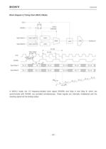
R CLK/2(Internal)Analog outInput Data AInput Data B DIV2INCLK DQQ Input Latch A Latch MUX Latch DAC Input Latch B Latch t > PD (B) Tpw1Tpw0t > PD (A) CLKInput Data AInput Data BNN + 1N 1N +1N + 3N + 5N + 7N֖ 2NN + 2N + 4N + 6 ts-DIV th-DIV01 2 3 tsDIV2IN th tdoN + 9N + 8 N + 2N + 3N + 4N + 5 tdo >
Open the catalog to page 25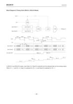
Latch Input Latch A Select Latch DAC Analog outInput Data AInput Data BC2CLK Input Latch B Tpw1Tpw0 t > PD (A) t > PD (B) CLK 1 ts-C2th-C2 1 C2 C2 Latch OUT Input Data AInput Data B N N 1N +1N + 3N + 5N + 7N֖ 2NN + 2N + 4N + 6 tdo N + 7N 2N֖ 4SELE. Atsth tdoN + 9N + 8SELE. BN + 2N + 5 >
Open the catalog to page 26All Sony Semiconductors catalogs and technical brochures
 IMX901-AMR
2 Pages
 IMX490
2 Pages
 IMX290NQV
2 Pages
 ISX016
2 Pages
 IMX390CQV
2 Pages
Archived catalogs
 SLD344YT
6 Pages
 SLD432S
5 Pages
 CXA3314ER
16 Pages
 CXB1818Q
17 Pages
 ICX205AK
24 Pages
 CXA2096N
17 Pages
 SLD433S4
5 Pages
 CXA4416GC
21 Pages
 CXA2984GC SP4T ANT SW
11 Pages
 SLD335YT
5 Pages
 CXM3807K
24 Pages
 CXM3648UR
11 Pages
 CXM3645ER
12 Pages
 CXM3642K
29 Pages
 CXM3641ER
22 Pages
 CXM3632ER
22 Pages
 CXM3630UR
15 Pages
 CXM3617ER
23 Pages
 CXM3614ER
14 Pages
 CXM3604UR
14 Pages
 CXM3599UR
15 Pages
 CXM3593UR
11 Pages
 SLD1332V
5 Pages
 CXM3592AUR
15 Pages
 CXM3583AUR
17 Pages
 CXM3582UR
17 Pages
 CXM3580UR
13 Pages
 CXM3580AUR
17 Pages
 CXM3572ER
14 Pages
 CXM3570ER
13 Pages
 CXM3569XR
13 Pages
 ICX418ALB
20 Pages
 CXD4728R
68 Pages
 ICX642BKA
23 Pages
 CXA3791EN
13 Pages
 SLD332F
6 Pages
 CXG1407XR
11 Pages
 IMX291LQR
2 Pages
 IMX252LLR/LQR
2 Pages
 IMX230
2 Pages
 IMX377CQT
5 Pages
 IMX249LLJ/LQJ
2 Pages
 IMX323LQN
2 Pages
 IMX258
2 Pages
 IMX302LQJ
2 Pages
 CXD4017R
34 Pages
 CXA3197R
30 Pages
 IMX222LQJ
2 Pages
 IMX324
2 Pages
 IMX367LLA
2 Pages
 IMX412-AACK
2 Pages
 IMX385LQR
2 Pages
 IMX294CJK
2 Pages
 IMX253LLR/LQR
2 Pages
 IMX273LLR/LQR
2 Pages
 IMX183CLK-J/CQJ-J
2 Pages
 IMX249LLJ/IMX249LQJ
2 Pages
 IMX250LLR/LQR,IMX252LLR/LQR
2 Pages
 B/W Video Camera CCD ICX422AL
17 Pages
 B/W Video Camera CCD ICX279AL*2
18 Pages
 Color Video Camera CCD ICX239AKE
18 Pages
 Color Video Camera CCD ICX418AKL
22 Pages


- Display module
- LCD display panel
- Color display panel
- LED display panel
- RGB display panel
- Compact display panel
- GNSS receiver
- Compact receiver
- Industrial receiver
- OLED display
- High-definition display module
- Laser diode
- Satellite receiver
- Sony CMOS image sensor
- Vision sensor
- Communication card
- Full HD display
- Fiber laser diode
- Sony visible image sensor
- Sony infrared image sensor