- Catalogs
- Sony Semiconductors
- ICX418ALB
- Products
- Catalogs
- News & Trends
- Exhibitions
ICX418ALB
1 /20Pages

ICX418ALB
1 /20Pages
Catalog excerpts
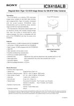
ICX418ALB Diagonal 8mm (Type 1/2) CCD Image Sensor for EIA B/W Video Cameras Description The ICX418ALB is an interline CCD solid-state image sensor suitable for EIA B/W video cameras with a diagonal 8mm (Type 1/2) system. Compared with the current product ICX038DLB, basic characteristics such as sensitivity, smear, dynamic range and S/N are improved drastically. This chip features a field period readout system and an electronic shutter with variable charge-storage time. Also, this outline is miniaturized by using original package. This chip is compatible with the pins of the ICX038DLB and has the same drive conditions. Features • High sensitivity (+5.0dB compared with the ICX038DLB) 3 • Low smear (–5.0dB compared with the ICX038DLB 40 H Pin 9 • High D range (+2.0dB compared with the ICX038DLB) • High S/N Optical black position • High resolution and low dark current (Top View) • Excellent antiblooming characteristics • Continuous variable-speed shutter • Substrate bias: Adjustment free (external adjustment also possible with 6 to 14V) • Reset gate pulse: 5Vp-p adjustment free (drive also possible with 0 to 9V) • Horizontal register: 5V drive • Maximum package dimensions: φ13.2mm Device Structure • Interline CCD image sensor • Optical size: Diagonal 8mm (Type 1/2) • Number of effective pixels: 768 (H) × 494 (V) approx. 380K pixels • Total number of pixels: 811 (H) × 508 (V) approx. 410K pixels • Chip size: 7.40mm (H) × 5.95mm (V) • Unit cell size: 8.4µm (H) × 9.8µm (V) • Optical black: Horizontal (H) direction: Front 3 pixels, rear 40 pixels Vertical (V) direction: Front 12 pixels, rear 2 pixels • Number of dummy bits: Horizontal 22 Vertical 1 (even fields only) • Substrate material: Silicon Sony reserves the right to change products and specifications without prior notice. This information does not convey any license by any implication or otherwise under any patents or other right. Application circuits shown, if any, are typical examples illustrating the operation of the devices. Sony cannot assume responsibility for any problems arising out of the use of these circuits.
Open the catalog to page 1
USE RESTRICTION NOTICE (December 1, 2003 ver.) This USE RESTRICTION NOTICE ("Notice") is for customers who are considering or currently using the CCD products ("Products") set forth in this specifications book. Sony Corporation ("Sony") may, at any time, modify this Notice which will be available to you in the latest specifications book for the Products. You should abide by the latest version of this Notice. If a Sony subsidiary or distributor has its own use restriction notice on the Products, such a use restriction notice will additionally apply between you and the subsidiary or distributor....
Open the catalog to page 2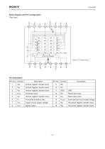
Vertical Register Block Diagram and Pin Configuration (Top View) Note) Horizontal Register : Photo sensor Vertical register transfer clock Vertical register transfer clock Vertical register transfer clock Substrate clock Reset drain bias Vertical register transfer clock Reset gate clock Protective transistor bias Substrate bias circuit supply voltage Output circuit supply voltage Horizontal register transfer clock Signal output Horizontal register transfer clock
Open the catalog to page 3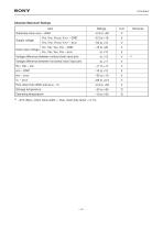
Absolute Maximum Ratings Item VDD, VRD, VDSUB, VOUT – φSUB Voltage difference between vertical clock input pins Voltage difference between horizontal clock input pins Pins other than GND and φSUB – VL Storage temperature Operating temperature Substrate clock φSUB – GND Supply voltage Clock input voltage ∗1 +27V (Max.) when clock width < 10µs, clock duty factor < 0.1%.
Open the catalog to page 4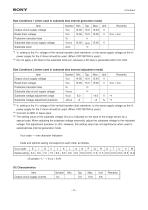
Bias Conditions 1 [when used in substrate bias internal generation mode] Item Output circuit supply voltage Reset drain voltage Protective transistor bias Substrate bias circuit supply voltage Substrate clock ∗1 VL setting is the VVL voltage of the vertical transfer clock waveform, or the same supply voltage as the VL power supply for the V driver should be used. (When CXD1267AN is used.) ∗2 Do not apply a DC bias to the substrate clock pin, because a DC bias is generated within the CCD. Bias Conditions 2 [when used in substrate bias external adjustment mode] Item Output circuit supply voltage...
Open the catalog to page 5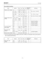
Clock Voltage Conditions Item Readout clock voltage Waveform diagram VφV Vertical transfer clock voltage High-level coupling High-level coupling Low-level coupling VVLL Horizontal transfer clock voltage Low-level coupling VRGLH – VRGLL Substrate clock voltage VφSUB VRGL Reset gate clock voltage∗1 Low-level coupling ∗1 Input the reset gate clock without applying a DC bias. In addition, the reset gate clock can also be driven with the following specifications. Item Reset gate clock voltage
Open the catalog to page 6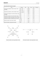
Clock Equivalent Circuit Constant Symbol Capacitance between horizontal transfer clock CφH1 and GND CφH2 Capacitance between horizontal transfer clocks Capacitance between reset gate clock and GND Capacitance between substrate clock and GND Capacitance between vertical transfer clock and GND Capacitance between vertical transfer clocks Vertical transfer clock series resistor Vertical transfer clock ground resistor Vertical transfer clock equivalent circuit Horizontal transfer clock equivalent circuit
Open the catalog to page 7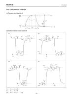
Drive Clock Waveform Conditions (1) Readout clock waveform 100% 90% (2) Vertical transfer clock waveform Vφ1 VVHL VVHL VVHL VVHL
Open the catalog to page 8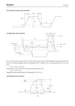
(3) Horizontal transfer clock waveform tr (4) Reset gate clock waveform VRGLH VRGL VRGLL VRGLm Hφ1 waveform +2.5V VRGLH is the maximum value and VRGLL is the minimum value of the coupling waveform during the period from Point A in the above diagram until the rising edge of RG. In addition, VRGL is the average value of VRGLH and VRGLL. VRGL = (VRGLH + VRGLL)/2 Assuming VRGH is the minimum value during the period twh, then: VφRG = VRGH – VRGL Negative overshoot level during the falling edge of RG is VRGLm. (5) Substrate clock waveform 100% 90%
Open the catalog to page 9All Sony Semiconductors catalogs and technical brochures
 IMX901-AMR
2 Pages
 IMX490
2 Pages
 IMX290NQV
2 Pages
 ISX016
2 Pages
 IMX390CQV
2 Pages
Archived catalogs
 SLD344YT
6 Pages
 SLD432S
5 Pages
 CXA3314ER
16 Pages
 CXB1818Q
17 Pages
 ICX205AK
24 Pages
 CXA2096N
17 Pages
 SLD433S4
5 Pages
 CXA4416GC
21 Pages
 CXA2984GC SP4T ANT SW
11 Pages
 SLD335YT
5 Pages
 CXM3807K
24 Pages
 CXM3648UR
11 Pages
 CXM3645ER
12 Pages
 CXM3642K
29 Pages
 CXM3641ER
22 Pages
 CXM3632ER
22 Pages
 CXM3630UR
15 Pages
 CXM3617ER
23 Pages
 CXM3614ER
14 Pages
 CXM3604UR
14 Pages
 CXM3599UR
15 Pages
 CXM3593UR
11 Pages
 SLD1332V
5 Pages
 CXM3592AUR
15 Pages
 CXM3583AUR
17 Pages
 CXM3582UR
17 Pages
 CXM3580UR
13 Pages
 CXM3580AUR
17 Pages
 CXM3572ER
14 Pages
 CXM3570ER
13 Pages
 CXM3569XR
13 Pages
 CXD4728R
68 Pages
 ICX642BKA
23 Pages
 CXA3791EN
13 Pages
 SLD332F
6 Pages
 CXG1407XR
11 Pages
 IMX291LQR
2 Pages
 IMX252LLR/LQR
2 Pages
 IMX230
2 Pages
 IMX377CQT
5 Pages
 IMX249LLJ/LQJ
2 Pages
 IMX323LQN
2 Pages
 IMX258
2 Pages
 IMX302LQJ
2 Pages
 CXD4017R
34 Pages
 CXA3197R
30 Pages
 IMX222LQJ
2 Pages
 IMX324
2 Pages
 IMX367LLA
2 Pages
 IMX412-AACK
2 Pages
 IMX385LQR
2 Pages
 IMX294CJK
2 Pages
 IMX253LLR/LQR
2 Pages
 IMX273LLR/LQR
2 Pages
 IMX183CLK-J/CQJ-J
2 Pages
 IMX249LLJ/IMX249LQJ
2 Pages
 IMX250LLR/LQR,IMX252LLR/LQR
2 Pages
 B/W Video Camera CCD ICX422AL
17 Pages
 B/W Video Camera CCD ICX279AL*2
18 Pages
 Color Video Camera CCD ICX239AKE
18 Pages
 Color Video Camera CCD ICX418AKL
22 Pages


- Liebherr display
- LCD display panel
- Color display panel
- LED display panel
- RGB display panel
- Compact display panel
- GNSS receiver
- Compact receiver
- Industrial receiver
- OLED display
- High-definition display module
- Laser diode
- Satellite receiver
- Liebherr CMOS image sensor
- Vision sensor
- Communication card
- Full HD display
- Fiber laser diode
- Codec
- Liebherr visible image sensor