- Catalogs
- Sony Semiconductors
- CXM3807K
- Products
- Catalogs
- News & Trends
- Exhibitions
CXM3807K
1 /24Pages

CXM3807K
1 /24Pages
Catalog excerpts
SP12T Antenna Switch Module for 10TRx/2Tx with MIPI I/F CXM3807K Description The CXM3807K is a SP12T antenna switch module for GSM/UMTS/CDMA/LTE multi-mode handset. The CXM3807K has a built-in dual low pass filter and a +1.8V CMOS compatible decoder with MIPI function. The Sony GaAs junction gate pHEMT (JPHEMT) MMIC process is used for low insertion loss. The device has low BOM with no DC blocking Capacitor. 0.55dB (Typ.) TRx (Cellular Band) 0.70dB (Typ.) TRx (IMT Tx Band) No DC Blocking Capacitors except sourcing DC bias Integration of ESD protection at Ant port Small Package Size: Lead-Free and RoHS Compliant Structure GaAs Junction Gate pHEMT (JPHEMT) MMIC Switch, CMOS Decoder This IC is ESD sensitive device. Special handling precautions are required.
Open the catalog to page 1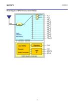
Block Diagram of SP12T Antenna Switch Module
Open the catalog to page 2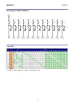
State Active Path
Open the catalog to page 3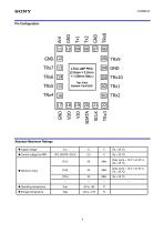
Absolute Maximum Ratings ◆ Supply voltage ◆ Control voltage for MIPI
Open the catalog to page 4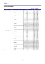
Electrical Characteristics Vdd=2.5V , Ta=25degC Item
Open the catalog to page 5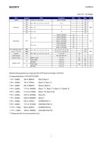
Path All Ports in Active Paths Inter modulation product pow er in Rx band Idd Supply current Ivio Control current SDATA, SCLK Active Mode Idle Mode Active Mode Idle Mode Electrical Characteristics are measured with all RF ports terminated in 50 Ohms. Corresponding Band of TRx(UMTS/CDMA) *1 Pin = 26dBm, (Band 1 Tx, Band 2 Tx, Band 3 Tx, Band4 Tx) *12 Measured with the recommended circuit
Open the catalog to page 7
Triple Beat Ratio (VDD = 2.5 V, Ta = 25 °C) Item Triple Beat Ratio Triple Beat Product *1 at TRx [MHz] Electrical characteristics are measured with all RF ports terminated in 50 . Measured with the recommended circuit Electrical characteristics are measured with all RF ports terminated in 50 . Measured with the recommended circuit
Open the catalog to page 9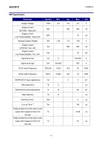
MIPI Specification Parameter Supply Voltage Supply current (ACTIVE) *Vdd=2.8V Supply current Low Power(disable) *Vdd=2.8V Interface Supply Voltage Supply current (ACTIVE) *Vio=1.8V Supply current Low Power(disable) *Vio=1.8V Signal level high SCLK write Frequency SCLK read Frequency SDATA/SCLK input capacitance Data setup time SDATA/SCLK load capacitance Data hold time Switching Time * Delay of data line at the slave’s pad output with respect to SCLK for full-rate Delay of data line at the slave’s pad output with respect to SCLK for half-rate
Open the catalog to page 10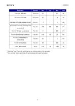
TSDataOTR (full-rate) TSDataOTR (half-rate) Interface OFF state leakage current VVIO-RST (final at powerdown) TVIO-RST(transitionary powerup) TVIO-RST(final phase) TSILOL (final phase) VVIO-RST(transitionary powerup and powerdown) TVIO-RST (transitionary at powerdown) * Switching Time: Timing for switching from an arbitrary state to the next state. **Turn on time: Time to guarantee RF performance after switch activation.
Open the catalog to page 11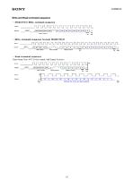
REGISTER_0 Write command sequence Write command sequence (except REGISTER_0) UE Address lAHfe Ccmmand Rente eir Addrcss - Read command sequence Data frame from ANT Switch needs Half Speed function Data frame Troni ANTSw Eel (Read Har Speed)
Open the catalog to page 13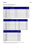
Register 0 write command sequence use. A Frame shall end with a single parity bit. The parity bit shall be driven such that the total number of bits in the Frame that are driven to logic level one. including the parity bit. is odd.
Open the catalog to page 14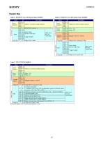
Table A REGISTERS for ANT Switch State (QxOOOO) Table B REGISTER.O for ANT Switch State (QxOOOO) All Data bits become 0 aftter Read Command Sequence is sent.
Open the catalog to page 15
Table G Register for Manufacturer ID (0x001 E) Table H Register for Manufacturer ID and USID (0x001 F) The PRODUCT ID and the MANUFACTURERS match, then a new USID is programmed.
Open the catalog to page 17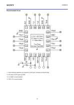
Bottom Pad:GND
Open the catalog to page 18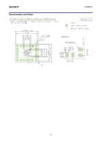
LTCC22 3.2x3,5 Macro drawing (Reference} 'PKG : 3.2ram>2.5uini t M a i a I mask -thickness : llQjim Mask (Open area) Resist (Open arsa)
Open the catalog to page 19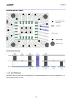
Cross section structure A note about PCB design Please keep distance TRx3(Pin22) line from SCLK(Pin21) and SDATA(Pin20) line in order to avoid the degradation for the harmonic performance of the TRx3. .
Open the catalog to page 20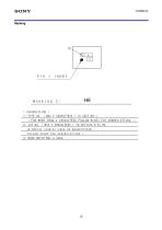
I) TYPE NO. ( MAX 2 CHARACTERS ) IN SECT IDN C._ ( FOR kORE THAN 2 CHARACTERS FOLLOW RULES FOR ABBREVI AT IQNS- ) FOLLOW RULES FOB ABBREVIATIONS- )
Open the catalog to page 22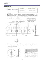
HATEBIAL = FQLViTTfll EHE "OhTMNlHG M BDhUHT I STATIC! (INTRODUCTION OF REUSE REEL KEEL THAT IS USED AGAIN AFTER COLLECTION) NE IPSE THE REUSE REEL OF JEITA SPECIFICATION.
Open the catalog to page 23
Note Sony reserves the right to change products and specifications without prior notice. This information does not convey any license by any implication or otherwise under any patents or other right. Application circuits shown, if any, are typical examples illustrating the operation of the devices. Sony cannot assume responsibility for any problems arising out of the use of these circuits
Open the catalog to page 24All Sony Semiconductors catalogs and technical brochures
 IMX901-AMR
2 Pages
 IMX490
2 Pages
 IMX290NQV
2 Pages
 ISX016
2 Pages
 IMX390CQV
2 Pages
Archived catalogs
 SLD344YT
6 Pages
 SLD432S
5 Pages
 CXA3314ER
16 Pages
 CXB1818Q
17 Pages
 ICX205AK
24 Pages
 CXA2096N
17 Pages
 SLD433S4
5 Pages
 CXA4416GC
21 Pages
 CXA2984GC SP4T ANT SW
11 Pages
 SLD335YT
5 Pages
 CXM3648UR
11 Pages
 CXM3645ER
12 Pages
 CXM3642K
29 Pages
 CXM3641ER
22 Pages
 CXM3632ER
22 Pages
 CXM3630UR
15 Pages
 CXM3617ER
23 Pages
 CXM3614ER
14 Pages
 CXM3604UR
14 Pages
 CXM3599UR
15 Pages
 CXM3593UR
11 Pages
 SLD1332V
5 Pages
 CXM3592AUR
15 Pages
 CXM3583AUR
17 Pages
 CXM3582UR
17 Pages
 CXM3580UR
13 Pages
 CXM3580AUR
17 Pages
 CXM3572ER
14 Pages
 CXM3570ER
13 Pages
 CXM3569XR
13 Pages
 ICX418ALB
20 Pages
 CXD4728R
68 Pages
 ICX642BKA
23 Pages
 CXA3791EN
13 Pages
 SLD332F
6 Pages
 CXG1407XR
11 Pages
 IMX291LQR
2 Pages
 IMX252LLR/LQR
2 Pages
 IMX230
2 Pages
 IMX377CQT
5 Pages
 IMX249LLJ/LQJ
2 Pages
 IMX323LQN
2 Pages
 IMX258
2 Pages
 IMX302LQJ
2 Pages
 CXD4017R
34 Pages
 CXA3197R
30 Pages
 IMX222LQJ
2 Pages
 IMX324
2 Pages
 IMX367LLA
2 Pages
 IMX412-AACK
2 Pages
 IMX385LQR
2 Pages
 IMX294CJK
2 Pages
 IMX253LLR/LQR
2 Pages
 IMX273LLR/LQR
2 Pages
 IMX183CLK-J/CQJ-J
2 Pages
 IMX249LLJ/IMX249LQJ
2 Pages
 IMX250LLR/LQR,IMX252LLR/LQR
2 Pages
 B/W Video Camera CCD ICX422AL
17 Pages
 B/W Video Camera CCD ICX279AL*2
18 Pages
 Color Video Camera CCD ICX239AKE
18 Pages
 Color Video Camera CCD ICX418AKL
22 Pages


- Liebherr display
- LCD display panel
- Color display panel
- LED display panel
- RGB display panel
- Compact display panel
- GNSS receiver
- Compact receiver
- Industrial receiver
- OLED display
- High-definition display module
- Laser diode
- Satellite receiver
- Liebherr CMOS image sensor
- Vision sensor
- Communication card
- Full HD display
- Fiber laser diode
- Codec
- Liebherr visible image sensor