- Catalogs
- Sony Semiconductors
- CXM3641ER
- Products
- Catalogs
- News & Trends
- Exhibitions
CXM3641ER
1 /22Pages

CXM3641ER
1 /22Pages
Catalog excerpts
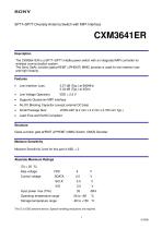
SP7T+SP7T Diversity Antenna Switch with MIPI Interface CXM3641ER Description The CXM3641ER is a SP7T+SP7T middle power switch with an integrated MIPI controller for wireless communication system. The Sony GaAs Junction gate pHEMT (JPHEMT) MMIC process is used for low insertion loss and high linearity. Features Supports Qualcomm MIPI interface No DC Blocking Capacitor (except external DC bias) Small Package Size: Lead-Free and RoHS Compliant Structure GaAs Junction gate pHEMT (JPHEMT) MMIC Switch, CMOS Decoder Moisture Sensitivity Moisture Sensitivity Level for this part is MSL = 2 Absolute Maximum Ratings (Ta = 25 ℃) Bias voltage Control voltage Input power max.(TRx) Operating temperature range Storage temperature range This IC is ESD sensitive device. Special handling precautions are required. 1
Open the catalog to page 1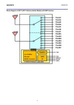
Level Shifter DCDC Converter CMOS Switch Controller
Open the catalog to page 2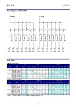
Truth Table HB SP7T (Register0) HB State State “L” means a switch “OFF”, state “H” means a switch “ON”.
Open the catalog to page 3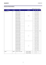
Electrical Characteristics (VDD = 2.5 V, Ta = 25 ℃) Parameter Insertion Loss All ports in active paths
Open the catalog to page 5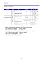
Electrical Characteristics (VDD = 2.5 V, Ta = 25 ℃) Parameter *3,*5 3fo IMD2 Inter Modulation Distortion Electrical Characteristics are measured with all RF ports terminated in 50 . * 1 Pin = 25dBm, 704 to 787 MHz (Band13, Band17) * 2 Pin = 26dBm, 824 to 960 MHz (Band1 Tx, Band 2 Tx, Band 3 Tx, Band 4 Tx) * 6 Measured with the recommended circuit.
Open the catalog to page 6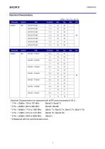
Electrical Characteristics (VDD = 2.5 V, Ta = 25 ℃) Parameter Electrical Characteristics are measured with all RF ports terminated in 50 . * 1 Pin = 25dBm, 704 to 787 MHz (Band13, Band17) * 2 Pin = 26dBm, 824 to 960 MHz (Band1 Tx, Band 2 Tx, Band 3 Tx, Band 4 Tx) * 6 Measured with the recommended circuit.
Open the catalog to page 7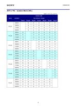
Isolation Matrix (Min.) (VDD = 2.5 V, Ta = 25 ℃) Isolation (dB) Path (ANTLB - TRxLB) TRxLB1
Open the catalog to page 8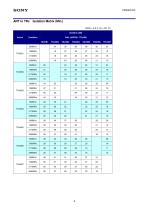
Isolation Matrix (Min.) (VDD = 2.5 V, Ta = 25 ℃) Isolation (dB) Path (ANTHB - TRxHB) TRxHB1
Open the catalog to page 9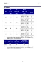
*Electrical characteristics are measured with all RF ports terminated in 50 . Measured with the recommended circuit f1 *Electrical characteristics are measured with all RF ports terminated in 50 . Measured with the recommended circuit
Open the catalog to page 10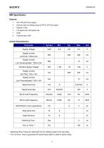
MIPI Specification Features PM_TRIG with three triggers Software reset and debug using the RFFE_STATUS register Full speed write, Half speed read Programmable USID Control Characteristics Supply Voltage Supply current (ACTIVE) *VDD=2.5V Supply current Low Power(disable) *VDD=2.5V Interface Supply Voltage Supply current (ACTIVE) *VIO=1.8V Supply current Low Power(disable) *VIO=1.8V Signal level high SCLK write Frequency SCLK read Frequency SDATA/SCLK input capacitance Data setup time Data hold time Switching Time * * Switching Time: Timing for switching from an arbitrary state to the next state....
Open the catalog to page 11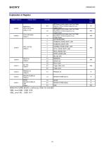
Explanation of Register Register Address Register Name Data Bits Read Write DATA_FRAME_PARITY_ERR READ_UNUSED_REG WRITE_UNUSED_REG HB Antenna sw itch states (see Truth Table) Register 0 Write command sequence use. Trigger Supprt. HB Antenna sw itch states (see Truth Table) Read/Write command sequence use. Trigger Supprt. LB Antenna sw itch states (see Truth Table) Read/Write command sequence use. Trigger Supprt. SOFTWARE RESET SPARE MANUFACTURER_ID USID (Table I) MANUFACTURER_ID[9:0] is defined by SONY ID (0x01B0) SSEL Level GND : USID 1010 SSEL Level VIO : USID 1011
Open the catalog to page 12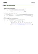
Write and Read command sequence - REGISTER_0 Write command sequence SCLK Slave Address - Write command sequence (except REGISTER_0) SCLK Slave Address Write Command Register Address - Read command sequence Data frame from ANT Switch needs Half Speed function ① Slave Address Read Command Register Address Data f rame f rom ANT Sw itch (Read Half Speed)
Open the catalog to page 13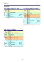
Command Frame Table B REGISTER_0 for HB ANT Switch State (0x0000) Items Bit Description SA3 1 Slave SA2 0 Address of Diversity Switch Address SA1 1 SA0 0/1 C2 0 Read Write : 010 C1 1 Write Read: 011 C0 0/1 A4 0 A3 0 Register A2 0 Register Address: 0x0000 Address A1 0 A0 0 Parity Bit P 0/1 Parity bit for Command Frame D7 0 D6 0 D5 0 Switch State Initial value : D4 0 See the truth table Data [D7:D0] D3 0 =0000 0000 D2 0/1 Trigger Supprt. D1 0/1 D0 0/1 Parity Bit P 0/1 Parity bit for Data Frame Data Frame Command Frame Table A REGISTER_0 for HB ANT Switch State (0x0000) Items Bit Description SA3...
Open the catalog to page 14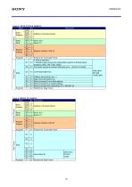
Command Frame (0x001A) Description Address of Diversity Switch Parity bit for Command Frame 0: Normal operation 0/1 1: Software reset (reset of all configurable registers to default values, except for USID、PM_TRIG、GSID) 0/1 Command sequence received with parity error – discard command. 0/1 Command length error Data Frame Command Frame Table E GROUP_ID Items SA3 Slave SA2 Address SA1 SA0 C2 Read C1 Write C0 A4 A3 Register A2 Address A1 A0 Parity Bit P Data Frame Address frame parity error = 1 Data frame with parity error Read command to an invalid address Write command to an invalid address Read...
Open the catalog to page 15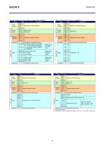
Command Frame Data Frame Data Frame Command Frame 0 0 0 Parity bit for Data Frame Data Frame Data Frame 0/1 Trigger_[2:0] 000: Invalid 0/1 other: valid 0/1 0/1 Parity bit for Data Frame Command Frame Table G Register for Product ID (0x001D) Items Description Bit SA3 1 Slave SA2 0 Address of Diversity Switch Address SA1 1 SA0 0/1 C2 0 Read C1 1 Read Only Write C0 1 A4 1 A3 1 Register A2 1 Register Address: 0x001D Address A1 0 A0 1 Parity Bit P 0/1 Parity bit for Command Frame D7 0 Command Frame Table F Register for Power Mode & Trigger Mode (0x001C) Items Description Bit SA3 1 Slave SA2 0 Address...
Open the catalog to page 16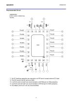
Recommended Circuit VQFN-24P PKG (2.4mm x 3.2mm x 0.725mm Typ.) Top View *1: No DC blocking capacitors are required on all RF ports (except external DC bias) *2: The DC levels of all RF ports are GND. *3: L1(27nH) and C1(12pF) are recommended on ANTHB port for ESD protection. *4: L2(27nH) and C2(12pF) are recommended on ANTLB port for ESD protection. *5: C3(100pF) and C4 (0.1uF) are recommended.
Open the catalog to page 17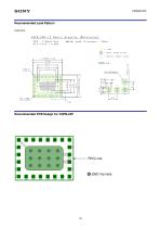
'GFN-24P-12 Macro drawing (Reference) * Metal mask "thickness : lOOjim Pj^ : Mask [Open area) J : Resist (Open area)
Open the catalog to page 18All Sony Semiconductors catalogs and technical brochures
 IMX901-AMR
2 Pages
 IMX490
2 Pages
 IMX290NQV
2 Pages
 ISX016
2 Pages
 IMX390CQV
2 Pages
Archived catalogs
 SLD344YT
6 Pages
 SLD432S
5 Pages
 CXA3314ER
16 Pages
 CXB1818Q
17 Pages
 ICX205AK
24 Pages
 CXA2096N
17 Pages
 SLD433S4
5 Pages
 CXA4416GC
21 Pages
 CXA2984GC SP4T ANT SW
11 Pages
 SLD335YT
5 Pages
 CXM3807K
24 Pages
 CXM3648UR
11 Pages
 CXM3645ER
12 Pages
 CXM3642K
29 Pages
 CXM3632ER
22 Pages
 CXM3630UR
15 Pages
 CXM3617ER
23 Pages
 CXM3614ER
14 Pages
 CXM3604UR
14 Pages
 CXM3599UR
15 Pages
 CXM3593UR
11 Pages
 SLD1332V
5 Pages
 CXM3592AUR
15 Pages
 CXM3583AUR
17 Pages
 CXM3582UR
17 Pages
 CXM3580UR
13 Pages
 CXM3580AUR
17 Pages
 CXM3572ER
14 Pages
 CXM3570ER
13 Pages
 CXM3569XR
13 Pages
 ICX418ALB
20 Pages
 CXD4728R
68 Pages
 ICX642BKA
23 Pages
 CXA3791EN
13 Pages
 SLD332F
6 Pages
 CXG1407XR
11 Pages
 IMX291LQR
2 Pages
 IMX252LLR/LQR
2 Pages
 IMX230
2 Pages
 IMX377CQT
5 Pages
 IMX249LLJ/LQJ
2 Pages
 IMX323LQN
2 Pages
 IMX258
2 Pages
 IMX302LQJ
2 Pages
 CXD4017R
34 Pages
 CXA3197R
30 Pages
 IMX222LQJ
2 Pages
 IMX324
2 Pages
 IMX367LLA
2 Pages
 IMX412-AACK
2 Pages
 IMX385LQR
2 Pages
 IMX294CJK
2 Pages
 IMX253LLR/LQR
2 Pages
 IMX273LLR/LQR
2 Pages
 IMX183CLK-J/CQJ-J
2 Pages
 IMX249LLJ/IMX249LQJ
2 Pages
 IMX250LLR/LQR,IMX252LLR/LQR
2 Pages
 B/W Video Camera CCD ICX422AL
17 Pages
 B/W Video Camera CCD ICX279AL*2
18 Pages
 Color Video Camera CCD ICX239AKE
18 Pages
 Color Video Camera CCD ICX418AKL
22 Pages


- Liebherr display
- LCD display panel
- Color display panel
- LED display panel
- RGB display panel
- Compact display panel
- GNSS receiver
- Compact receiver
- Industrial receiver
- OLED display
- High-definition display module
- Laser diode
- Satellite receiver
- Liebherr CMOS image sensor
- Vision sensor
- Communication card
- Full HD display
- Fiber laser diode
- Codec
- Liebherr visible image sensor