- Catalogs
- Sony Semiconductors
- CXM3632ER
- Products
- Catalogs
- News & Trends
- Exhibitions
CXM3632ER
1 /22Pages

CXM3632ER
1 /22Pages
Catalog excerpts
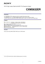
SP10T High Linearity Switch with MIPI I/F for Qualcomm chipset CXM3632ER Description The CXM3632ER is SP10T middle power switch for wireless communication system. The CXM3632ER has a 1.8 V CMOS compatible decoder with MIPI function for Qualcomm chipset. The SONY GaAs junction gate pHEMT(JPHEMT) MMIC process is used for low insertion loss and high linearity. Features ◆Low Insertion loss : 0.38 dB(typ.) at GSM Low Band, UMTS BAND 5 0.46 dB(typ.) at GSM High Band, UMTS BAND 1 ◆Low Voltage Operation : VDD = 2.5 V ◆No DC Blocking Capacitors (except sourcing DC bias) ◆Supports CMOS control for serial interface(MIPI I/F for Qualcomm chipset) ◆Small package Size : VQFN-20pin (2.4 mm × 2.4 mm × 0.725 mm Typ.) ◆Lead-Free and RoHS compliant Structure GaAs Junction Gate pHEMT(JPHEMT) MMIC switch, CMOS decoder This IC is ESD sensitive device. Special handling precautions are required.
Open the catalog to page 1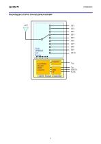
Level Shifter CMOS Switch Controller
Open the catalog to page 2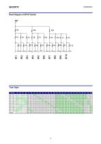
Block Diagram of SP10T Switch
Open the catalog to page 3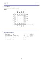
Absolute Maximum Ratings ◆ Supply voltage ◆ Control voltage for MIPI
Open the catalog to page 4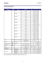
Electrical Characteristics (VDD = 2.5 V, Ta = 25 ℃) Param eter Insertion Loss 3fo Inter Modulation Distortion in Rx Band All ports in active paths Active Mode Idle Mode Idle Mode Control Current Supply Current Ivio Electrical characteristics are measured with all RF ports terminated in 50 .
Open the catalog to page 5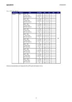
ANT – RF1 (Active Ports RF4/5/6/7/8/9/10) ANT – RF2 (Active Ports RF4/5/6/7/8/9/10) Electrical characteristics are measured with all RF ports terminated in 50 .
Open the catalog to page 6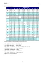
ANT to RF Isolation Matrix Active Electrical characteristics are measured with all RF ports terminated in 50 . (Band1 Tx, Band 2 Tx, Band 3 Tx, Band 4 Tx) * 8 Measured with the recommended circuit.
Open the catalog to page 7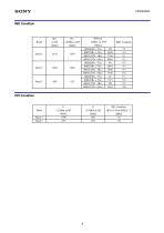
Band Band 1 Band 5
Open the catalog to page 8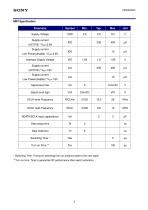
MIPI Specification Parameter Supply Voltage Supply current (ACTIVE) *VDD=2.8V Supply current Low Power(disable) *VDD=2.8V Interface Supply Voltage Supply current (ACTIVE) *VIO=1.8V Supply current Low Power(disable) *VIO=1.8V Signal level high SCLK write Frequency SCLK read Frequency SDATA/SCLK input capacitance Data setup time Data hold time Switching Time * * Switching Time: Timing for switching from an arbitrary state to the next state. **Turn on time: Time to guarantee RF performance after switch activation.
Open the catalog to page 9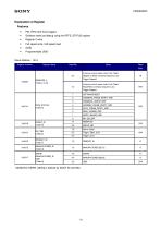
Explanation of Register Features PM_TRIG with three triggers Software reset and debug using the RFFE_STATUS register Full speed write, half speed read Programmable USID Slave Address : 1010. Register Address Register Name Data Bits Read Write Antenna sw itch states (see Truth Table) Register 0 Write command sequence use. Trigger Support. Antenna sw itch states (see Truth Table) Read/Write command sequence use. Trigger Support. SOFTWARE RESET SPARE MANUFACTURER_ID USID (Table H)
Open the catalog to page 10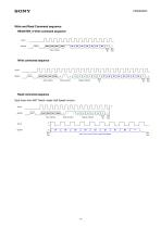
Write and Read Command sequence REGISTER_0 Write command sequence Slave Address Write command sequence Slave Address Write Command Register Address Read command sequence Data frame from ANT Switch needs Half Speed function. ① Slave Address Read Command Register Address Data frame from ANT Sw itch (Read Half Speed)
Open the catalog to page 11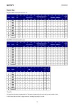
Register Map Register 0 Write command sequence use. 24 Slave Address Register Address Read/Write command sequence use. 24 Slave Address Register Address *Parity Bit A Frame shall end with a single parity bit. The parity bit shall be driven such that the total number of bits in the Frame that are driven to logic level one, including the parity bit, is odd.
Open the catalog to page 12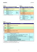
Items Slave Address Address of Diversity Switch REGISTER_0 Write : 1 Switch State See the truth table Trigger Supprt. Command Frame Read Write Register Address Parity Bit Data Frame Command Frame Table B REGISTER_0 for ANT Switch State (0x0000) Description Address of Diversity Switch Write : 010 Read: 011 Register Address: 0x0000 Parity bit for Command Frame Switch State See the truth table Trigger Supprt. Parity bit for Data Frame Table C RFFE_STATUS (0x001A) Items Command Frame Slave Address Read Write Register Address Data Frame Description Bit SA3 1 SA2 0 Address of Diversity Switch SA1 1...
Open the catalog to page 13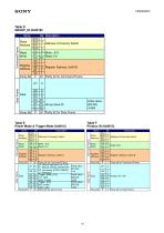
Command Frame Slave Address Read Write Register Address Parity Bit Data Frame Table E Power Mode & Trigger Mode (0x001C) Command Frame Slave Address Read Write Register Address Data Frame Register Address Parity Bit Initial value : [D7:D6] =10 Initial value : [D5:D3] =000 Initial value : [D5:D3] =000 Read Write Slave Address Command Frame Data Frame Address of Diversity Switch Read Only Register Address: 0x001D Parity bit for Command Frame
Open the catalog to page 14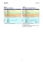
Table G Manufacturer ID (0x001E) Items Table H Manufacturer ID and USID (0x001F) Description Slave Address Address of Diversity Switch Command Frame Command Frame Register Address Read Write Slave Address Read Only Register Address: 0x001E Parity bit for Command Frame Read Write Register Address Parity Bit Data Frame Data Frame SPARE 1 Manufacturer ID [7:0]:B0h (SONY ID) 1 0 0 0 0 0 Parity bit for Data Frame 0 Manufacturer ID [9:8]:01h (SONY ID) 1 0/1 Initial 0/1 Programmable USID value:[D3:D0] 0/1 =1010 0/1 0/1 Parity bit for Data Frame For Programmable USID The PRODUCT_ID and the MANUFACTURER_ID...
Open the catalog to page 15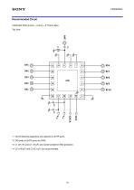
Recommended Circuit VQFN-20P PKG (2.4mm × 2.4mm × 0.775mm Max.) Top View *1: No DC blocking capacitors are required on all RF ports. *2: DC levels of all RF ports are GND. *3: L1 (27 nH) and C1 (15 pF) are recommended for ESD protection. *4: C2 (100 pF) and C3 (0.1 µF) are recommended.
Open the catalog to page 16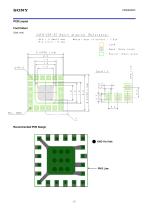
VQFN-gDP-07 Macro drawing (Reference) ■PKG : 2.4mmXP.4.rnm tMela I mask thickness : MO.urn
Open the catalog to page 17
1] LflT IIC. < HJ.lt i CUHCTHi : SEHIH CODE I IH SECTION B._ l ftLurn tuLfs rot ^BBHEvi AT I rma._ HMWfUCTLUlNC mt IS DltFUYEIt BY FOLLMlIMC BYHftKY BIT 5Y5TEH. ) > flU CCDEi TIE HT IIT OF * ftlUAHV SYSTEM BIT 5Y5TEH IS DlifUtEC IN I IDT I IN 1ECTI0H i- ii mt mil m iho BIT OF n t\uti SYSTEM BIT SYSTEH IS pismttt IN I POT UH SECTian I. > mi tatu in «p air OF K t\mi STSTEN BIT SYSTEM IS PI smut IN I tor >m SECT I BH C. jj cam in <ii in OF A imtar SYSTEM BIT STSTFJM IS Disfmut IN I tor >m Simon t. I w mint ru,N 3 CMJUACTEH^ FHIQI MULES FPH ^BBEEYHTIONB. )_
Open the catalog to page 19All Sony Semiconductors catalogs and technical brochures
 IMX901-AMR
2 Pages
 IMX490
2 Pages
 IMX290NQV
2 Pages
 ISX016
2 Pages
 IMX390CQV
2 Pages
Archived catalogs
 SLD344YT
6 Pages
 SLD432S
5 Pages
 CXA3314ER
16 Pages
 CXB1818Q
17 Pages
 ICX205AK
24 Pages
 CXA2096N
17 Pages
 SLD433S4
5 Pages
 CXA4416GC
21 Pages
 CXA2984GC SP4T ANT SW
11 Pages
 SLD335YT
5 Pages
 CXM3807K
24 Pages
 CXM3648UR
11 Pages
 CXM3645ER
12 Pages
 CXM3642K
29 Pages
 CXM3641ER
22 Pages
 CXM3630UR
15 Pages
 CXM3617ER
23 Pages
 CXM3614ER
14 Pages
 CXM3604UR
14 Pages
 CXM3599UR
15 Pages
 CXM3593UR
11 Pages
 SLD1332V
5 Pages
 CXM3592AUR
15 Pages
 CXM3583AUR
17 Pages
 CXM3582UR
17 Pages
 CXM3580UR
13 Pages
 CXM3580AUR
17 Pages
 CXM3572ER
14 Pages
 CXM3570ER
13 Pages
 CXM3569XR
13 Pages
 ICX418ALB
20 Pages
 CXD4728R
68 Pages
 ICX642BKA
23 Pages
 CXA3791EN
13 Pages
 SLD332F
6 Pages
 CXG1407XR
11 Pages
 IMX291LQR
2 Pages
 IMX252LLR/LQR
2 Pages
 IMX230
2 Pages
 IMX377CQT
5 Pages
 IMX249LLJ/LQJ
2 Pages
 IMX323LQN
2 Pages
 IMX258
2 Pages
 IMX302LQJ
2 Pages
 CXD4017R
34 Pages
 CXA3197R
30 Pages
 IMX222LQJ
2 Pages
 IMX324
2 Pages
 IMX367LLA
2 Pages
 IMX412-AACK
2 Pages
 IMX385LQR
2 Pages
 IMX294CJK
2 Pages
 IMX253LLR/LQR
2 Pages
 IMX273LLR/LQR
2 Pages
 IMX183CLK-J/CQJ-J
2 Pages
 IMX249LLJ/IMX249LQJ
2 Pages
 IMX250LLR/LQR,IMX252LLR/LQR
2 Pages
 B/W Video Camera CCD ICX422AL
17 Pages
 B/W Video Camera CCD ICX279AL*2
18 Pages
 Color Video Camera CCD ICX239AKE
18 Pages
 Color Video Camera CCD ICX418AKL
22 Pages


- Liebherr display
- LCD display panel
- Color display panel
- LED display panel
- RGB display panel
- Compact display panel
- GNSS receiver
- Compact receiver
- Industrial receiver
- OLED display
- High-definition display module
- Laser diode
- Satellite receiver
- Liebherr CMOS image sensor
- Vision sensor
- Communication card
- Full HD display
- Fiber laser diode
- Codec
- Liebherr visible image sensor