- Catalogs
- Sony Semiconductors
- CXM3617ER
- Products
- Catalogs
- News & Trends
- Exhibitions
CXM3617ER
1 /23Pages

CXM3617ER
1 /23Pages
Catalog excerpts
SP14T Antenna Switch Module for 12TRx/2Tx with MIPI I/F for Qualcomm chipset The CXM3617ER is a SP14T antenna switch module for GSM / UMTS / CDMA / LTE multi-mode handset. The CXM3617ER has a +1.8 V CMOS compatible decoder with MIPI function for Qualcomm chipset. The Sony GaAs junction gate pHEMT (JPHEMT) MMIC process is used for low insertion loss and high linearity. The device has low BOM with no DC blocking Capacitor. (Applications: GSM/TD-SCDMA/WCDMA/LTE multi-mode handset) 0.50 dB (Typ.) TRx (Cellular Band) 0.70 dB (Typ.) TRx (IMT Tx Band) Supports CMOS control for serial interface (MIPI I/F for Qualcomm chipset) Small Package Size: Lead-Free and RoHS Compliant Structure GaAs Junction Gate pHEMT (JPHEMT) MMIC Switch, CMOS Decoder This IC is ESD sensitive device. Special handling precautions are required. Sony reserves the right to change products and specifications without prior notice. This information does not convey any license by any implication or otherwise under any patents or other right. Application circuits shown, if any, are typical examples illustrating the operation of the devices. Sony cannot assume responsibility for any problems arising out of the use of these circuits
Open the catalog to page 1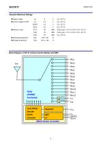
Absolute Maximum Ratings ◆ Supply voltage ◆ Control voltage for MIPI Block Diagram of SP14T Antenna Switch Module with MIPI Level Shifter Decoder DC/DC Converter CMOS Switch Controller
Open the catalog to page 2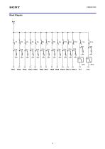
Block Diagram
Open the catalog to page 3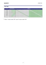
Truth Table State *1) State “L” means a switch “OFF”, state “H” means a switch “ON”.
Open the catalog to page 4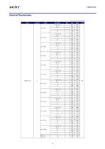
Electrical Characteristics VDD = 2.5 V, Ta = 25 ˚C Item Insertion Loss
Open the catalog to page 6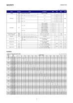
All Ports in Active Paths Wakeup Time Supply Current SCLK falling edge to 90% RF in Active Mode From Low Pow er Mode to Active Mode Inter Modulation Product Pow er in Rx Band
Open the catalog to page 7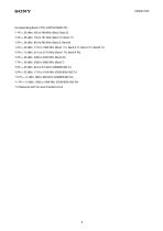
Corresponding Band of TRx (UMTS/CDMA/LTE) *1 Pin = 26 dBm, 452 to 468 MHz (Band Class 5) *2 Pin = 25 dBm, 704 to 787 MHz (Band 13, Band 17) *3 Pin = 26 dBm, 824 to 960 MHz (Band 5, Band 8) *4 Pin = 26 dBm, 1710 to 1990 MHz (Band 1 Tx, Band 2 Tx, Band 3 Tx, Band4 Tx) *5 Pin = 10 dBm, 2110 to 2170 MHz (Band 1 Rx, Band 4 Rx) *6 Pin = 26 dBm, 2300 to 2400 MHz (Band 40) *7 Pin = 26 dBm, 2500 to 2690 MHz (Band 7) *8 Pin = 35 dBm, 824 to 915 MHz (GSM850/900 Tx) *9 Pin = 32 dBm, 1710 to 1910 MHz (GSM1800/1900 Tx) *10 Pin = 10 dBm, 869 to 960 MHz (GSM850/900 Rx) *11 Pin = 10 dBm, 1805 to 1990 MHz (GSM1800/1900...
Open the catalog to page 8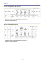
Electrical Characteristics of Triple Beat Ratio VDD = 2.5 V, Ta = 25 °C Condition Item Triple Beat Ratio Triple Beat Product at TRx [MHz] Electrical characteristics are measured with all RF ports terminated in 50 . Measured with the recommended circuit Electrical Characteristics of Input IP2 VDD = 2.5 V, Ta = 25 °C Condition Electrical characteristics are measured with all RF ports terminated in 50 . Measured with the recommended circuit
Open the catalog to page 10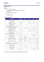
MIPI Specification Features PM_TRIG with three triggers Software reset and debug using the RFFE_STATUS register Full speed write, Half speed read Programmable USID Control Characteristics Supply Voltage Signal level high SCLK write Frequency SCLK read Frequency SDATA/SCLK input capacitance Data setup time Data hold time Supply current (ACTIVE) *VDD = 2.5 V Supply current Low Power(disable) *VDD = 2.5 V Interface Supply Voltage Supply current (ACTIVE) *VIO = 1.8 V Supply current Low Power(disable) *VIO = 1.8 V *Turn on time: Time to guarantee RF performance after switch activation.
Open the catalog to page 11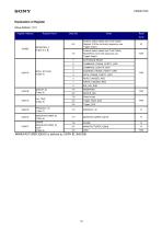
Explanation of Register Slave Address: 1011 Register Address Register Name Data Bits Read Write Antenna switch states (see Truth Table) Register 0 Write command sequence use. Trigger Supprt. Antenna switch states (see Truth Table) Read/Write command sequence use. Trigger Supprt. DATA_FRAME_PARITY_ERR READ_UNUSED_REG Power mode SOFTWARE RESET SPARE MANUFACTURER_ID USID (Table H)
Open the catalog to page 12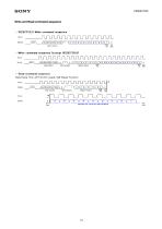
REGISTER_0 Write command sequence Btauc Address „ „ „ Write command sequence (except REGISTER_0) Seue Addrcff 'A* Ife Command Rent fcr Addreff — Read command sequence Data frame from ANT Switch needs Half Speed function Data Trame from ANTSw Eel (Read Har Speed)
Open the catalog to page 13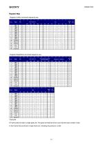
Register Map Register 0 Write command sequence use. 15 Slave Address Register Read/Write command sequence use. 24 Slave Address Register Address *Parity Bit A Frame shall end with a single parity bit. The parity bit shall be driven such that the total number of bits in the Frame that are driven to logic level one, including the parity bit, is odd.
Open the catalog to page 14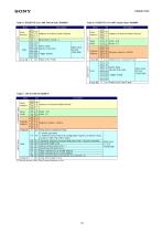
Table A REGISTER 0 fbr AWT Switch State (OxOOOO) Table B REGISTER 0 fbr AMT Switch State (OxOOOO) All Data bits become 0 aftter Read Command Sequence is sent.
Open the catalog to page 15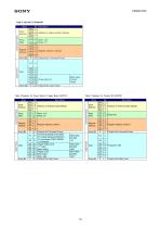
Table E Register for Power Mode & Trigger Mode (0x001C) Read Write Register Address Data Frame Register Address Parity Bit Initial value : [D7:D6] =10 Initial value : [D5:D3] =000 Initial value : [D2:D0] =000 Read Write Slave Address Command Frame Command Frame Slave Address Data Frame Table F Register for Product ID (0x001D) Address of Antenna Switch Module Read Only Parity bit for Command Frame Parity bit for Data Frame
Open the catalog to page 16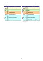
Table G Register for Manufacturer ID (0x001E) Table H Register for Manufacturer ID and USID (0x001F) Address of Antenna Switch Module Slave Address Command Frame Register Address Parity Bit Read Write 1 Manufacturer ID [7:0]:B0h (SONY ID) 1 0 0 0 0 0 Parity bit for Data Frame Command Frame Slave Address Read Only Parity bit for Command Frame Read Write Register Address Parity Bit Data Frame Data Frame 0 Manufacturer ID [9:8]:01h (SONY ID) 1 0/1 0/1 Programmable USID 0/1 0/1 0/1 Parity bit for Data Frame For Programmable USID The PRODUCT_ID and the MANUFACTURER_ID match, then a new USID is programmed....
Open the catalog to page 17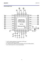
Recommended Circuit *1: No DC blocking capacitors are required on all RF ports. *2: DC levels of all RF ports are GND. *3: L1 (22 nH) and C1 (22 pF) are recommended on Ant port for ESD protection. *4: C2 (100 pF) and C3 (0.1 µF) are recommended.
Open the catalog to page 18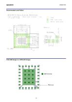
VQFN-26P-02 Macro drawing (Reference) ■Pin pitch : Q.dmm HH : Mask (Open area) : Resist (Open area)
Open the catalog to page 19All Sony Semiconductors catalogs and technical brochures
 IMX901-AMR
2 Pages
 IMX490
2 Pages
 IMX290NQV
2 Pages
 ISX016
2 Pages
 IMX390CQV
2 Pages
Archived catalogs
 SLD344YT
6 Pages
 SLD432S
5 Pages
 CXA3314ER
16 Pages
 CXB1818Q
17 Pages
 ICX205AK
24 Pages
 CXA2096N
17 Pages
 SLD433S4
5 Pages
 CXA4416GC
21 Pages
 CXA2984GC SP4T ANT SW
11 Pages
 SLD335YT
5 Pages
 CXM3807K
24 Pages
 CXM3648UR
11 Pages
 CXM3645ER
12 Pages
 CXM3642K
29 Pages
 CXM3641ER
22 Pages
 CXM3632ER
22 Pages
 CXM3630UR
15 Pages
 CXM3614ER
14 Pages
 CXM3604UR
14 Pages
 CXM3599UR
15 Pages
 CXM3593UR
11 Pages
 SLD1332V
5 Pages
 CXM3592AUR
15 Pages
 CXM3583AUR
17 Pages
 CXM3582UR
17 Pages
 CXM3580UR
13 Pages
 CXM3580AUR
17 Pages
 CXM3572ER
14 Pages
 CXM3570ER
13 Pages
 CXM3569XR
13 Pages
 ICX418ALB
20 Pages
 CXD4728R
68 Pages
 ICX642BKA
23 Pages
 CXA3791EN
13 Pages
 SLD332F
6 Pages
 CXG1407XR
11 Pages
 IMX291LQR
2 Pages
 IMX252LLR/LQR
2 Pages
 IMX230
2 Pages
 IMX377CQT
5 Pages
 IMX249LLJ/LQJ
2 Pages
 IMX323LQN
2 Pages
 IMX258
2 Pages
 IMX302LQJ
2 Pages
 CXD4017R
34 Pages
 CXA3197R
30 Pages
 IMX222LQJ
2 Pages
 IMX324
2 Pages
 IMX367LLA
2 Pages
 IMX412-AACK
2 Pages
 IMX385LQR
2 Pages
 IMX294CJK
2 Pages
 IMX253LLR/LQR
2 Pages
 IMX273LLR/LQR
2 Pages
 IMX183CLK-J/CQJ-J
2 Pages
 IMX249LLJ/IMX249LQJ
2 Pages
 IMX250LLR/LQR,IMX252LLR/LQR
2 Pages
 B/W Video Camera CCD ICX422AL
17 Pages
 B/W Video Camera CCD ICX279AL*2
18 Pages
 Color Video Camera CCD ICX239AKE
18 Pages
 Color Video Camera CCD ICX418AKL
22 Pages


- Liebherr display
- LCD display panel
- Color display panel
- LED display panel
- RGB display panel
- Compact display panel
- GNSS receiver
- Compact receiver
- Industrial receiver
- OLED display
- High-definition display module
- Laser diode
- Satellite receiver
- Liebherr CMOS image sensor
- Vision sensor
- Communication card
- Full HD display
- Fiber laser diode
- Codec
- Liebherr visible image sensor