- Catalogs
- Sony Semiconductors
- CXM3593UR
- Products
- Catalogs
- News & Trends
- Exhibitions
CXM3593UR
1 /11Pages

CXM3593UR
1 /11Pages
Catalog excerpts
High Power DPDT Switch CXM3593UR Description The CXM3593UR is a high power DPDT switch for wireless communication systems. This IC has a 1.8 V CMOS compatible decoder. The Sony GaAs junction gate pHEMT (JPHEMT) MMIC process is used for low insertion loss and high linearity. (Application: LTE/CDMA/GSM/UMTS Handsets ) Features ◆ Low Insertion loss: 0.26dB (Typ.) (Cellular Band ) 0.45 dB (Typ.) (IMT2000 ) ◆ Low voltage operation: VDD = 2.5 V ◆ No DC blocking capacitors required on RF ports ◆ 2 Control input ◆ Small package size: UQFN-12 pin (2.0 mm × 2.0 mm) ◆ Lead-Free and RoHS compliant Structure GaAs JPHEMT MMIC switch, CMOS decoder Moisture Sensitivity Moisture Sensitivity Level for this part is MSL= 2 (Tentative) Absolute Maximum Ratings ♦ Bias voltage ♦ Maximum input power This IC is ESD sensitive device. Special handling precautions are required. 1
Open the catalog to page 1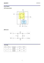
Block Diagram DPDT Antenna Switch RF3 Decoder Logic MMIC Switch Active path
Open the catalog to page 2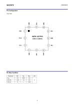
DC Bias Condition Parameter
Open the catalog to page 3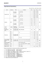
Target Electrical Characteristics (Ta = 25 °C, VDD = 2.5 V, Vctl = 0/1.8 V) Item Insertion Loss All ports in active paths Inter modulation distortion in Rx Band Switching speed Wakeup time Control current Supply current Electrical characteristics are measured with all RF ports terminated in 50 Ω. *1 *2 *3 *4 *5 *6 *7 *8 *9 *10 Pin = 25 dBm, 704 to 787 MHz (Band 13, Band 17) Pin = 26 dBm, 824 to 960 MHz (Band 5, Band 8) Pin = 26 dBm, 1710 to 1990 MHz (Band 1 Tx, Band 2 Tx, Band 3 Tx, Band 4 Tx) Pin = 10 dBm, 2110 to 2170 MHz (Band 1 Rx, Band 4 Rx) Pin = 26 dBm, 2500 to 2690 MHz (Band 7) Pin =...
Open the catalog to page 4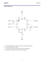
Recommended Circuit *1 No DC blocking capacitors are required on all RF ports. (Except sourcing DC bias) *2 The DC levels of all RF ports are GND. *3 L1 (27nH) and C1(12pF) are recommended on Ant port for ESD protection. *4 C2(100pF) is recommended on VDD pin for Decoupling Capacitor.
Open the catalog to page 6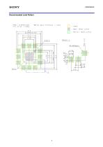
Recommended Land Pattern
Open the catalog to page 7
MNJFAnOAlNi f EAR IS DISPLAYED S V FOLLOW INS Bimi E IT SVSTEH, * YEAR <ME\ THE 1ST EIT IF * BIHAR* SlSTEH HI T SYSTEM IS NSPLAYEj t> V E-flN C l> U E '- THE 2 \ 3 HIT JF » BIHAR' S "If S T EM JIT SVoTEM IS UjPLAYEI IN I OH I IN SECT 101 I:. * YEAR CC-CE C THE JB] E IT ]F <> BINAR* 5"V&TEH 31T SYSTEM IS CISPLAYE] IN I OCT I IN SECT 101 c A V EAR CDCE ( THE 4TH EIT ]F A BINARY SKSTEH 3IT 3 V 5 FEN IS CISPLVfE] IN I DCT 1 IN SECT 101 d- F:IK HQHE TH.^N ■ ::HAHftCTEKS FOLLD'H HJLE^ F^ ftHhHEvI*TI:
Open the catalog to page 9
lATEll I.L:FDLTSTTEEHE CMTJIIIl£ CAP.HDH IAHTIJT.'TI [I [REEL THAT \$ USEE AGAIN AFTER COLLECTION) tfE USE THE REUSE (EEL OF JEIT* OPEC IFICATIDM-
Open the catalog to page 10
Note Sony reserves the right to change products and specifications without prior notice. This information does not convey any license by any implication or otherwise under any patents or other right. Application circuits shown, if any, are typical examples illustrating the operation of the devices. Sony cannot assume responsibility for any problems arising out of the use of these circuits.
Open the catalog to page 11All Sony Semiconductors catalogs and technical brochures
 IMX901-AMR
2 Pages
 IMX490
2 Pages
 IMX290NQV
2 Pages
 ISX016
2 Pages
 IMX390CQV
2 Pages
Archived catalogs
 SLD344YT
6 Pages
 SLD432S
5 Pages
 CXA3314ER
16 Pages
 CXB1818Q
17 Pages
 ICX205AK
24 Pages
 CXA2096N
17 Pages
 SLD433S4
5 Pages
 CXA4416GC
21 Pages
 CXA2984GC SP4T ANT SW
11 Pages
 SLD335YT
5 Pages
 CXM3807K
24 Pages
 CXM3648UR
11 Pages
 CXM3645ER
12 Pages
 CXM3642K
29 Pages
 CXM3641ER
22 Pages
 CXM3632ER
22 Pages
 CXM3630UR
15 Pages
 CXM3617ER
23 Pages
 CXM3614ER
14 Pages
 CXM3604UR
14 Pages
 CXM3599UR
15 Pages
 SLD1332V
5 Pages
 CXM3592AUR
15 Pages
 CXM3583AUR
17 Pages
 CXM3582UR
17 Pages
 CXM3580UR
13 Pages
 CXM3580AUR
17 Pages
 CXM3572ER
14 Pages
 CXM3570ER
13 Pages
 CXM3569XR
13 Pages
 ICX418ALB
20 Pages
 CXD4728R
68 Pages
 ICX642BKA
23 Pages
 CXA3791EN
13 Pages
 SLD332F
6 Pages
 CXG1407XR
11 Pages
 IMX291LQR
2 Pages
 IMX252LLR/LQR
2 Pages
 IMX230
2 Pages
 IMX377CQT
5 Pages
 IMX249LLJ/LQJ
2 Pages
 IMX323LQN
2 Pages
 IMX258
2 Pages
 IMX302LQJ
2 Pages
 CXD4017R
34 Pages
 CXA3197R
30 Pages
 IMX222LQJ
2 Pages
 IMX324
2 Pages
 IMX367LLA
2 Pages
 IMX412-AACK
2 Pages
 IMX385LQR
2 Pages
 IMX294CJK
2 Pages
 IMX253LLR/LQR
2 Pages
 IMX273LLR/LQR
2 Pages
 IMX183CLK-J/CQJ-J
2 Pages
 IMX249LLJ/IMX249LQJ
2 Pages
 IMX250LLR/LQR,IMX252LLR/LQR
2 Pages
 B/W Video Camera CCD ICX422AL
17 Pages
 B/W Video Camera CCD ICX279AL*2
18 Pages
 Color Video Camera CCD ICX239AKE
18 Pages
 Color Video Camera CCD ICX418AKL
22 Pages


- Liebherr display
- LCD display panel
- Color display panel
- LED display panel
- RGB display panel
- Compact display panel
- GNSS receiver
- Compact receiver
- Industrial receiver
- OLED display
- High-definition display module
- Laser diode
- Satellite receiver
- Liebherr CMOS image sensor
- Vision sensor
- Communication card
- Full HD display
- Fiber laser diode
- Codec
- Liebherr visible image sensor