- Catalogs
- Sony Semiconductors
- CXM3582UR
- Products
- Catalogs
- News & Trends
- Exhibitions
CXM3582UR
1 /17Pages

CXM3582UR
1 /17Pages
Catalog excerpts
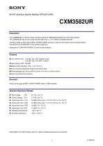
SP10T Antenna Switch Module 6TRx/2Tx/2Rx CXM3582UR Description The CXM3582UR is a SP10T antenna switch module for GSM/UMTS/CDMA/LTE multi-mode handset. The CXM3582UR has a built-in dual low pass filter and a +1.8 V CMOS compatible decoder. The Sony GaAs junction gate pHEMT (JPHEMT) MMIC process is used for low insertion loss and high linearity. The device has low BOM with no DC blocking capacitor. (Applications: GSM/UMTS/CDMA/LTE multi-mode handsets) Features ◆ Low insertion loss: 0.45 dB (Typ.) TRx (Cellular band) 0.60 dB (Typ.) TRx (IMT Tx band) ◆ High linearity: IIP3 = 68 dBm ◆ Battery direct operation: VDD = 2.5 V to 5.0 V ◆ No DC blocking capacitors except sourcing DC bias ◆ Small package size: 26-pin UQFN (2.6 mm x 3.4 mm x 0.625 mm Max.) ◆ Lead-free and RoHS compliant Structure GaAs junction gate pHEMT (JPHEMT) MMIC switch, CMOS decoder Absolute Maximum Ratings ◆ Bias voltage GaAs MMIC’s are ESD sensitive devices. Special handling precautions are required.
Open the catalog to page 1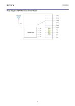
Block Diagram of SP10T Antenna Switch Module
Open the catalog to page 2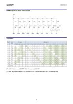
Truth Table State Active path (*1) State “L” means a switch “OFF”, State “H” means a switch “ON” (*2) State “Idle” means that the DC/DC converter is “OFF”, and the switch paths are in an undefined state.
Open the catalog to page 3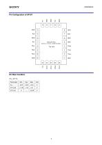
DC Bias Condition (Ta = 25 °C) Parameter
Open the catalog to page 4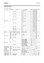
Target Specification (VDD = 2.5 V, Ta = 25 °C) Item All ports in active paths Inter modulation product power in Rx band Input IP3 Switching time Control current Supply current Supply current *12A, 25, 26 50 % Ctl to 90 % RF Wake up time from Idle mode to Active mode VCTL = 1.80 V VDD = 2.8 V VDD = 2.8 V Active mode Idle mode
Open the catalog to page 5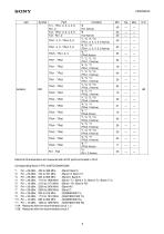
Electrical Characteristics are measured with all RF ports terminated in 50 Ω. Corresponding Band of TRx (UMTS/CDMA/GSM) *1 Pin = 26 dBm, 452 to 468 MHz (Band Class 5) *2 Pin = 25 dBm, 704 to 787 MHz (Band 13, Band 17) *3 Pin = 26 dBm, 824 to 960 MHz (Band 5, Band 8) *4 Pin = 26 dBm, 1710 to 1990 MHz (Band 1 Tx, Band 2 Tx, Band 3 Tx, Band 4 Tx) *5 Pin = 10 dBm, 2110 to 2170 MHz (Band 1 Rx, Band 4 Rx) *6 Pin = 26 dBm, 2300 to 2400 MHz (Band 40) *7 Pin = 26 dBm, 2500 to 2690 MHz (Band 7) *8 Pin = 35 dBm, 824 to 915 MHz (GSM850/900 Tx) *9 Pin = 32 dBm, 1710 to 1910 MHz (GSM1800/1900 Tx) *10 Pin =...
Open the catalog to page 6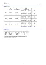
IIP3 Condition Band Band I Band V Electrical Characteristics are measured with all RF ports terminated in 50 Ω. Measured with the recommended circuit.
Open the catalog to page 7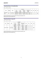
Target Specification of Triple Beat Ratio (VDD = 2.5V, Ta = 25 °C) Condition Item Triple beat ratio Jammer Triple beat Min. at Ant product –30 dBm at TRx* 881.5 MHz 881.5 ± 1 MHz 81 Electrical Characteristics are measured with all RF ports terminated in 50 Ω. Measured with the recommended circuit Target Specification of Input IP2 (VDD = 2.5 V, Ta = 25 °C) Electrical Characteristics are measured with all RF ports terminated in 50 Ω. Measured with the recommended circuit
Open the catalog to page 8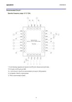
*1: No DC blocking capacitors are required on all RF ports. (Except sourcing DC bias) *2: DC levels of all RF ports are GND. *3: L1 (22 nH) and C1 (22 pF) are recommended on Ant port for ESD protection. *4: C2 capacitor (100 pF) is recommended. *5: TRx5 is recommended for Band7. Operation frequency range: 0.7-2.7 GHz
Open the catalog to page 9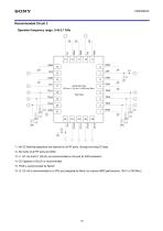
Operation frequency range: 0.45-2.7 GHz *1: No DC blocking capacitors are required on all RF ports. (Except sourcing DC bias) *2: DC levels of all RF ports are GND. *3: L1 (47 nH) and C1 (22 pF) are recommended on Ant port for ESD protection. *4: C2 Capacitor (100 pF) is recommended. *5: TRx5 is recommended for Band7. *6: L2 (12 nH) is recommended on a TRx port assigned for Band I to improve IMD2 performance. (Rx-Tx (190 MHz))
Open the catalog to page 10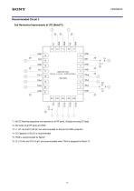
*1: No DC blocking capacitors are required on all RF ports. (Except sourcing DC bias) *2: DC levels of all RF ports are GND. *3: L1 (47 nH) and C1(22 pF) are recommended on Ant port for ESD protection. *4: C2 Capacitor (100 pF) is recommended. *5: TRx5 is recommended for Band7. *6: L2 (1.8 nH) and C3 (4.0 pF) are recommended when TRx4 is assigned for Band 13.
Open the catalog to page 11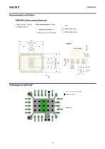
Recommended Land Pattern UQFN-26P-01 Macro drawing (Reference) PKG: 3.4 mm x 2.6 mm * Metal mask thickness: 110 µm : Mask (Open area) : Metal area in board (*1) : Resist (Open area)
Open the catalog to page 12
I) LOT NO. ( MAX 3 CHARACTERS ■ SERIAL CODE ) IN SECTION B._ ( FOLLOW RULES FOR ABBREVIATIONS._ MANUFACTURING YEAR IS DISPLAYED BY FOLLOWING BYNARY BIT SYSTEM. ) A YEAR CDDE1 THE 1ST BIT OF A BINARY SYSTEM BIT SYSTEM IS DISPLAYED IN I DOT )IN SECTION a. A YEAR CODE ( THE 2ND BIT OF A BINARY SYSTEM BIT SYSTEM IS DISPLAYED IN I DOT )IN SECTION b. A YEAR CODE( THE 3RD BIT OF A BINARY SYSTEM BIT SYSTEM IS DISPLAYED IN I DOT )IN SECTION c. A YEAR CODE ( THE 4TH BIT OF A BINARY SYSTEM BIT SYSTEM IS DISPLAYED IN 1 DOT )IN SECTION d. 2) TYPE NO. ( MAX 5 CHARACTERS ) IN SECTION C._ ( FOR MORE THAN 5 CHARACTERS...
Open the catalog to page 15
I) LOT NO. ( MAX 3 CHARACTERS = SERIAL CODE ) IN SECTION B._ ( FOLLOW RULES FOR ABBREVIATIONS._ MANUFACTURING YEAR IS DISPLAYED BY FOLLOWING BYNARY BIT SYSTEM. ) A YEAR CODE t THE 1ST BIT OF A BINARY SYSTEM BIT SYSTEM IS DISPLAYED IN I DOT )IN SECTION a. A YEAR CODE ( THE 2ND BIT OF A BINARY SYSTEM BIT SYSTEM IS DISPLAYED IN I DOT ) IN SECTION b. A YEAR CODE ( THE 3RD BIT OF A BINARY SYSTEM BIT SYSTEM IS DISPLAYED IN I DOT ) IN SECTION c. A YEAR CODE ( THE 4TH BIT OF A BINARY SYSTEM BIT SYSTEM IS DISPLAYED IN I DOT ) IN SECTION d. 2) TYPE NO. ( MAX 5 CHARACTERS ) IN SECTION C._ ( FOR MORE THAN...
Open the catalog to page 16
Note Sony reserves the right to change products and specifications without prior notice. This information does not convey any license by any implication or otherwise under any patents or other right. Application circuits shown, if any, are typical examples illustrating the operation of the devices. Sony cannot assume responsibility for any problems arising out of the use of these circuits.
Open the catalog to page 17All Sony Semiconductors catalogs and technical brochures
 IMX901-AMR
2 Pages
 IMX490
2 Pages
 IMX290NQV
2 Pages
 ISX016
2 Pages
 IMX390CQV
2 Pages
Archived catalogs
 SLD344YT
6 Pages
 SLD432S
5 Pages
 CXA3314ER
16 Pages
 CXB1818Q
17 Pages
 ICX205AK
24 Pages
 CXA2096N
17 Pages
 SLD433S4
5 Pages
 CXA4416GC
21 Pages
 CXA2984GC SP4T ANT SW
11 Pages
 SLD335YT
5 Pages
 CXM3807K
24 Pages
 CXM3648UR
11 Pages
 CXM3645ER
12 Pages
 CXM3642K
29 Pages
 CXM3641ER
22 Pages
 CXM3632ER
22 Pages
 CXM3630UR
15 Pages
 CXM3617ER
23 Pages
 CXM3614ER
14 Pages
 CXM3604UR
14 Pages
 CXM3599UR
15 Pages
 CXM3593UR
11 Pages
 SLD1332V
5 Pages
 CXM3592AUR
15 Pages
 CXM3583AUR
17 Pages
 CXM3580UR
13 Pages
 CXM3580AUR
17 Pages
 CXM3572ER
14 Pages
 CXM3570ER
13 Pages
 CXM3569XR
13 Pages
 ICX418ALB
20 Pages
 CXD4728R
68 Pages
 ICX642BKA
23 Pages
 CXA3791EN
13 Pages
 SLD332F
6 Pages
 CXG1407XR
11 Pages
 IMX291LQR
2 Pages
 IMX252LLR/LQR
2 Pages
 IMX230
2 Pages
 IMX377CQT
5 Pages
 IMX249LLJ/LQJ
2 Pages
 IMX323LQN
2 Pages
 IMX258
2 Pages
 IMX302LQJ
2 Pages
 CXD4017R
34 Pages
 CXA3197R
30 Pages
 IMX222LQJ
2 Pages
 IMX324
2 Pages
 IMX367LLA
2 Pages
 IMX412-AACK
2 Pages
 IMX385LQR
2 Pages
 IMX294CJK
2 Pages
 IMX253LLR/LQR
2 Pages
 IMX273LLR/LQR
2 Pages
 IMX183CLK-J/CQJ-J
2 Pages
 IMX249LLJ/IMX249LQJ
2 Pages
 IMX250LLR/LQR,IMX252LLR/LQR
2 Pages
 B/W Video Camera CCD ICX422AL
17 Pages
 B/W Video Camera CCD ICX279AL*2
18 Pages
 Color Video Camera CCD ICX239AKE
18 Pages
 Color Video Camera CCD ICX418AKL
22 Pages


- Liebherr display
- LCD display panel
- Color display panel
- LED display panel
- RGB display panel
- Compact display panel
- GNSS receiver
- Compact receiver
- Industrial receiver
- OLED display
- High-definition display module
- Laser diode
- Satellite receiver
- Liebherr CMOS image sensor
- Vision sensor
- Communication card
- Full HD display
- Fiber laser diode
- Codec
- Liebherr visible image sensor