- Catalogs
- Sony Semiconductors
- CXM3569XR
- Products
- Catalogs
- News & Trends
- Exhibitions
CXM3569XR
1 /13Pages

CXM3569XR
1 /13Pages
Catalog excerpts
SP4T Antenna Switch for GSM / CDMA / UMTS CXM3569XR Description The CXM3569XR is a high power SP4T antenna switch for GSM / CDMA / UMTS applications. The antenna port can be routed to either of the 4TRx ports. The low insertion loss on transmit means increased talk time as the Tx power amplifier can be operated at a lower output level. Built-in decoder reduces component count and simplifies PCB layout by allowing direct connection of the switch to digital base band control lines with the 1.8 V CMOS logic levels. The Sony GaAs JPHEMT MMIC Process is used for low insertion loss and high linearity. Features ◆ Low Insertion Loss: 0.31 dB typical (Cellular / GSM Low Band) 0.41 dB typical (PCS / GSM High Band) 0.46 dB typical (IMT2000) ◆ No DC Blocking Capacitors Required on RF ports. ◆ Small Package Size: ◆ Lead-Free and RoHS Compliant Structure GaAs JPHEMT MMIC Absolute Maximum Ratings ◆ Bias Voltage ◆ Maximum input power ◆ Storage Temperature ◆ Maximum power dissipation ◆ Copper-clad lamination of glass board(4 layer) *NOTICE Please use this product without exceeding PD value showed on it's specification. If it is used with exceeding PD value even for a moment, there are possibilities of degradation or breakdown because of the heat generated by product operation. GaAs MMICs are ESD sensitive devices. Special handling precautions are required.
Open the catalog to page 1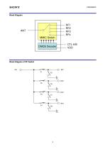
Block Diagram CMOS Decoder Block Diagram of RF Switch
Open the catalog to page 2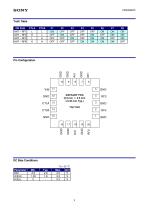
Truth Table ON Path CTLA ANT – RF1 L ANT – RF2 H ANT – RF3 L ANT – RF4 H Parameter Vdd Vctl(H) Vctl(L)
Open the catalog to page 3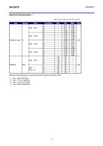
Electrical Characteristics 1 Vdd = 2.5 V, Vctl = 0/1.8 V Ta = 25 °C Electrical Characteristics are measured with all RF ports terminated in 50 Ω. *1 *2 *3 *4 freq = 698 to 960 MHz freq = 1710 to 1990 MHz freq = 2110 to 2170 MHz freq = 2500 to 2690 MHz
Open the catalog to page 4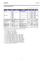
Electrical Characteristics 2 Vdd = 2.5 V, Vctl = 0/1.8 V Ta = 25 °C Item VSWR P0.2dB Compression Inter Modulation Product Power in Rx Band Control Current Supply Current Switching Time Wakeup Time 824 to 1980 MHz *5 -*8, *15 *9 -*12, *15 *13, *15 *14, *15 Vctl = 1.8 V per line Vdd = 2.5 V 50 % Ctl to 90 % RF Wakeup time from Vdd on to Active mode Electrical Characteristics are measured with all RF ports terminated in 50 Ω. Corresponding Band of TRx (UMTS/CDMA) *1 *2 *3 *4 *5 *6 *7 *8 *9 * 10 * 11 * 12 * 13 * 14 * 15 Pin = 35 dBm, freq = 824 to 915 MHz Pin = 32 dBm, freq = 1710 to 1910 MHz Pin...
Open the catalog to page 5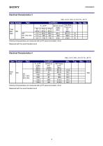
Electrical Characteristics 3 Vdd = 2.5 V, Vctl = 0/1.8 V Ta = 25 °C Item Symbol Triple Beat Ratio Triple Beat Product at RF* [MHz] 881.5±1 1960±1 2132±1 Electrical Characteristics are measured with all RF ports terminated in 50 Ω. Measured with the recommended circuit Electrical Characteristics 4 Vdd = 2.5 V, Vctl = 0/1.8 V Ta = 25 °C Item Symbol Electrical Characteristics are measured with all RF ports terminated in 50 Ω. Measured with the recommended circuit
Open the catalog to page 6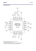
Recommended Circuit 1: No DC blocking capacitors are required on all RF ports. *2: DC levels of all RF ports are GND. *3: L1(39 nH) and C1(15 pF) are recommended on Ant port for ESD protection. *4: C2(100 pF) is recommended on Vdd pin for Decoupling Capacitor.
Open the catalog to page 7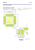
Recommended Land Pattern XQFN-20P-02 Macro for MMIC ・PKG Size□2.5mm×t0.35mm ・Terminal Pitch0.4mm :Land area :Board resist open area :Mask open area (Solder printing area) :Metal area in board (*1)
Open the catalog to page 8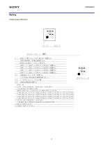
aSfi$3- K (2 l;£b-y h 7^(7)1 b'7 hgfrj^) frEMTS. bSEfrJ - K (2il£b''y hfiafl2b'-y hBft&iO EElta. I) LOT NO. I Ut 3 CHARACTERS ■ SERIAL CODE ) IN SECTION B,_ [ FOLLOW RULES FOB ABBREVIATIONS._ MANUFACTURING YEAR IS DISPLAYED BY FOLLOW ING BYNARY BIT SYSTEM. ) A YEAR CODE I THE 1ST BIT OF A BINARY SYSTEM BIT SYSTEM IS DISPLAYED IN I DOT )IN SECTION a. A YEAR CODEI THE 2ND BIT OF A BINARY SYSTEM BIT SYSTEM IS DISPLAYED IN I DOT )IN SECTION b. A YEAR CODE ( THE 3RD BIT OF A BINARY SYSTEM BIT SYSTEM IS DISPLAYED IN I DOT )IN SECTION c. A YEAR CODE I THE 4TH BIT OF A BINARY SYSTEM BIT SYSTEM IS DISPLAYED...
Open the catalog to page 11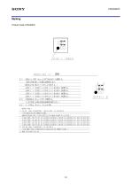
agEgD- (21£tf-vl-J)ji^1 b'-^B*^) £KITj>. II LOT NO. ( MAX 3 CHARACTERS ■ SERIAL CODE ) IN SECTION 8._ I FOLLOW RULES FOR ABBREVIATIONS._ KAKUFACTURING YEftR IS DISPLACED BY FDLLOWIHC BYNARY BIT SY5TEH. ) A YEfiR CO0EI THE 1ST BIT 3T A BINARY SYSTEM BIT SYSTEM IS DISPLACED IN I OPT TIN SECTION a. A YEAR CODEI THE 2ND BIT OF A BINARY SYSTEM BIT SYSTEM IS DISPLAYED III I OPT TIN SECTION t. A 1EAR CODE! THE 3RD BIT Of A BINARY SYSTEM BIT SYSTEM IS DISPLACED IN I DOT TIN SECTION c. A YEAR CODE I TIE 4TH BIT OF A BINARY SYSTEM BIT SYSTEM IS DISPLACED IN I DOT TIN SECTION d. 21 TYPE NO. I HAY 1 CHARACTERS...
Open the catalog to page 12
Note Sony reserves the right to change products and specifications without prior notice. This information does not convey any license by any implication or otherwise under any patents or other right. Application circuits shown, if any, are typical examples illustrating the operation of the devices. Sony cannot assume responsibility for any problems arising out of the use of these circuits
Open the catalog to page 13All Sony Semiconductors catalogs and technical brochures
 IMX901-AMR
2 Pages
 IMX490
2 Pages
 IMX290NQV
2 Pages
 ISX016
2 Pages
 IMX390CQV
2 Pages
Archived catalogs
 SLD344YT
6 Pages
 SLD432S
5 Pages
 CXA3314ER
16 Pages
 CXB1818Q
17 Pages
 ICX205AK
24 Pages
 CXA2096N
17 Pages
 SLD433S4
5 Pages
 CXA4416GC
21 Pages
 CXA2984GC SP4T ANT SW
11 Pages
 SLD335YT
5 Pages
 CXM3807K
24 Pages
 CXM3648UR
11 Pages
 CXM3645ER
12 Pages
 CXM3642K
29 Pages
 CXM3641ER
22 Pages
 CXM3632ER
22 Pages
 CXM3630UR
15 Pages
 CXM3617ER
23 Pages
 CXM3614ER
14 Pages
 CXM3604UR
14 Pages
 CXM3599UR
15 Pages
 CXM3593UR
11 Pages
 SLD1332V
5 Pages
 CXM3592AUR
15 Pages
 CXM3583AUR
17 Pages
 CXM3582UR
17 Pages
 CXM3580UR
13 Pages
 CXM3580AUR
17 Pages
 CXM3572ER
14 Pages
 CXM3570ER
13 Pages
 ICX418ALB
20 Pages
 CXD4728R
68 Pages
 ICX642BKA
23 Pages
 CXA3791EN
13 Pages
 SLD332F
6 Pages
 CXG1407XR
11 Pages
 IMX291LQR
2 Pages
 IMX252LLR/LQR
2 Pages
 IMX230
2 Pages
 IMX377CQT
5 Pages
 IMX249LLJ/LQJ
2 Pages
 IMX323LQN
2 Pages
 IMX258
2 Pages
 IMX302LQJ
2 Pages
 CXD4017R
34 Pages
 CXA3197R
30 Pages
 IMX222LQJ
2 Pages
 IMX324
2 Pages
 IMX367LLA
2 Pages
 IMX412-AACK
2 Pages
 IMX385LQR
2 Pages
 IMX294CJK
2 Pages
 IMX253LLR/LQR
2 Pages
 IMX273LLR/LQR
2 Pages
 IMX183CLK-J/CQJ-J
2 Pages
 IMX249LLJ/IMX249LQJ
2 Pages
 IMX250LLR/LQR,IMX252LLR/LQR
2 Pages
 B/W Video Camera CCD ICX422AL
17 Pages
 B/W Video Camera CCD ICX279AL*2
18 Pages
 Color Video Camera CCD ICX239AKE
18 Pages
 Color Video Camera CCD ICX418AKL
22 Pages


- Liebherr display
- LCD display panel
- Color display panel
- LED display panel
- RGB display panel
- Compact display panel
- GNSS receiver
- Compact receiver
- Industrial receiver
- OLED display
- High-definition display module
- Laser diode
- Satellite receiver
- Liebherr CMOS image sensor
- Vision sensor
- Communication card
- Full HD display
- Fiber laser diode
- Codec
- Liebherr visible image sensor