- Catalogs
- Sony Semiconductors
- CXD4728R
- Products
- Catalogs
- News & Trends
- Exhibitions
CXD4728R
1 /68Pages

CXD4728R
1 /68Pages
Catalog excerpts
intelligent Panel Controller for Standard Frame Rate System CXD4728R Description The CXD4728R is an image signal processor for Flat Panel Display system, which can improve a quality of color representation, contrast feeling, and resolution feeling. This LSI has some unique features; the function “Bi-axial Color Control” that improves a quality of color representation by changing colors on x-y chromaticity graph. The method of color adjustment is easier and the operability is improved compared to the general Hue adjustment. The function “intelligent Contrast Synthesizer” improves the contrast feelings and resolution feeling. Especially a contrast for the dark scene is improved. This function is realized only by signal processing, and it does not depend on back-light system. The function “Two Dimensions Sharpness” improves sharpness and spacial effect. And two sets of 12-bit RGB independent gamma compensation can change the gamma curve and white balance. Those functions can adjust a picture depending on user's liking or characteristics of various panels. The connection to a customer system is easy and also the picture adjustment is easy by small registers. It is not needed to largely reconstruct existing system software. (Applications: Color TFT-LCD TV, Panel Module) Features Bi-axial Color Control Function intelligent Contrast Synthesizer Function 2D Sharpness Function Brightness, Color, Contrast Control Double Gamma Correction with full-size 12-bit RGB independent LUT Dither function for 8-bit panel system LVDS Receiver and Transmitter which support single/dual links 8-bit Rigor 10-bit RGB Input/Output frequency range 65MHz to 85MHz (SS included) Tolerates Spread Spectrum Clock at the LVDS input SSCG (spread spectrum clock generator) for LVDS Tx clock Support display resolutions WXGA (1366 768p) or Full-HD (1920 1080p) I2C Slave Interface for external host CPU (100kHz to 400kHz) I2C Master Interface for stand-alone startup with max. 128K-bit external EEPROM (optional). No need external DRAM Support Support Structure Silicon gate CMOS IC Sony reserves the right to change products and specifications without prior notice. This information does not convey any license by any implication or otherwise under any patents or other right. Application circuits shown, if any, are typical examples illustrating the operation of the devices. Sony cannot assume responsibility for any problems arising out of the use of these circuits. -1- E10418-PS
Open the catalog to page 1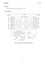
CXD4728R Package LQFP 128 pins (0.5mm pin pitch, body size 20mm 14mm) 1. Block Diagram intelligent Image Processor RXBCK (Clock) PLL B DE Clock Clock R G B DE Register Interface Block I2C Slave Interface I2C Master Interface Clock Circuits I2C Bus Through Path SCL/SDA 2 bits Slave Address Selector Host I/F SCL/SDA Master Address Selector Master Busy Signal Clock Input Reset Input 20MHz to 30MHz (25MHz for I2C Master I/F use) EEPROM for start-up (Optional) Fig.1-1. intelligent Panel Controller Block Diagram -2- TXA0 to TXA4 (8 bits/10 bits) 5ch LVDS Tx SSCG PLL 5ch LVDS Tx G DE Dither 5ch LVDS...
Open the catalog to page 2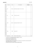
*! Unused pins must be fixed to High (3.3V) or OPEN for LVDS Rx. *2 Unused pins must be OPEN for LVDS Tx. *3 Active Low reset is required after turn On. *4 The external pull-up registers are required. *5 At the release of RST_X, if the IIC_MST_EN pin is High, the IIC_SLV_BUSY pin becomes High till l2C Master Reading Operation is completed. *6 Exposed Pad must be connected to GND and soldered to PCB.
Open the catalog to page 7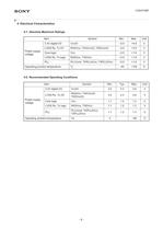
4-1. Absolute Maximum Ratings 4-2. Recommended Operating Conditions
Open the catalog to page 8
4-3-1. Digital In/Out Terminal *2 IIC_MST_SDA, IIC_SLV_SDA, IIC_MST_EN, IIC_MST_SADSEL, IIC_SLV_SADSEL0, *4 1.2V VDD includes RXDVDD, TXPLLAVDD, TXPLLDVDD, TXDVDD, PLLVDDA, VDD *5 3.3V VDD includes RXAVDD, TXAVDD33, TXDVDD33, VDDIO *2 VCM : LVDS common voltage *2 RL: Load condition, ILVDS: LVDS driver current on LVDS Tx bus
Open the catalog to page 9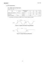
4-4-1. System Clock and Reset Input *l It is desirable to set frequency to 25MHz if the l2C master interface is enabled. Fig.4-4-1-1. System Clock SCLKI Timing Definition Fig.4-4-1-2. System Reset Input Waveform
Open the catalog to page 10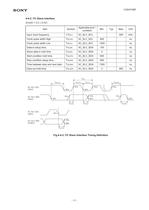
Fig.4-4-2.12C Slave Interface Timing Definition
Open the catalog to page 11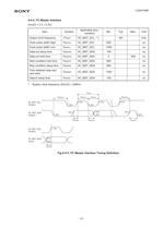
*! System clock frequency (SCLKI) = 25MHz Fig.4-4-3.12C Master Interface Timing Definition
Open the catalog to page 12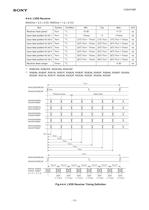
*! RXBCKN, RXBCKP, RXACKN, RXACKP Previous Cycle Next Cycle RXAXP RXBXP _m ffl^_W W_W W_MA +/—TRSKM +/-TRSKM +/-TRSKM +/-TRSKM +/-TRSKM +/-TRSKM +/-TRSKM Fig.4-4-4. LVDS Receiver Timing Definition
Open the catalog to page 13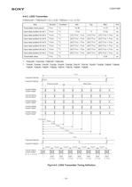
*! TXACKP, TXACKN, TXBCKP, TXBCKN Previous Cycle Next Cycle +/—TTSK +/-TTSK +/-TTSK +/-TTSK +/-TTSK +/-TTSK +/-TTSK Fig.4-4-5. LVDS Transmitter Timing Definition
Open the catalog to page 14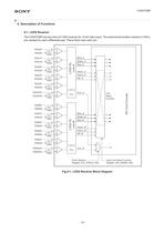
The CXD4728R has two links of LVDS receiver for 10-bit video input. The external termination resistors (100Q) are needed for each differential pair. Place them near each pin. Clock Selector Input Link Swap Function Register CLK_RXCLK_SEL Register VIN_LNKMS_SEL Fig.5-1. LVDS Receiver Block Diagram
Open the catalog to page 15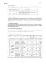
This LSI supports two video formats as follows. That mode is applied to both LVDS Rx and Tx. To change the mode, see "7-5. Standard Register Settings" of later description. 5-1-2. Link Swap Function The LVDS Rx link swap function can replace Link-B with Link-A. For single link (WXGA), choose Link-A or B by this function. If Link-Bis used, change the link by the VIN_LNKMS_SEL register (Page 1Ah, Address OOh, Bit [1]). For dual link (Full-HD), 1st link (1, 3, 5, 1919) and 2nd link (2, 4, 6, 1920) can be swapped by this function. 5-1-3. Video Clock Selector One of LVDS Rx links is selected for the...
Open the catalog to page 16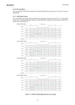
This LSI operates in the DE-only mode and only Data Enable (DE) is used for sync. H sync and V sync are 5-1-7. LVDS Data Format This LSI supports two modes, VESA and JEIDA. Bit assignment is shown in the Fig.5-1-7. To change this format, see "7-5. Standard Register Settings" of later description. Selected format is applied to both Link A Format: VESA, 8 bits Current Cycle Format: VESA, 10 bits Current Cycle Format: JEIDA, 8 bits Current Cycle Format: JEIDA, 10 bits Current Cycle Fig.5-1-7. LVDS Formats (Reserved bit is not used)
Open the catalog to page 17All Sony Semiconductors catalogs and technical brochures
 IMX901-AMR
2 Pages
 IMX490
2 Pages
 IMX290NQV
2 Pages
 ISX016
2 Pages
 IMX390CQV
2 Pages
Archived catalogs
 SLD344YT
6 Pages
 SLD432S
5 Pages
 CXA3314ER
16 Pages
 CXB1818Q
17 Pages
 ICX205AK
24 Pages
 CXA2096N
17 Pages
 SLD433S4
5 Pages
 CXA4416GC
21 Pages
 CXA2984GC SP4T ANT SW
11 Pages
 SLD335YT
5 Pages
 CXM3807K
24 Pages
 CXM3648UR
11 Pages
 CXM3645ER
12 Pages
 CXM3642K
29 Pages
 CXM3641ER
22 Pages
 CXM3632ER
22 Pages
 CXM3630UR
15 Pages
 CXM3617ER
23 Pages
 CXM3614ER
14 Pages
 CXM3604UR
14 Pages
 CXM3599UR
15 Pages
 CXM3593UR
11 Pages
 SLD1332V
5 Pages
 CXM3592AUR
15 Pages
 CXM3583AUR
17 Pages
 CXM3582UR
17 Pages
 CXM3580UR
13 Pages
 CXM3580AUR
17 Pages
 CXM3572ER
14 Pages
 CXM3570ER
13 Pages
 CXM3569XR
13 Pages
 ICX418ALB
20 Pages
 ICX642BKA
23 Pages
 CXA3791EN
13 Pages
 SLD332F
6 Pages
 CXG1407XR
11 Pages
 IMX291LQR
2 Pages
 IMX252LLR/LQR
2 Pages
 IMX230
2 Pages
 IMX377CQT
5 Pages
 IMX249LLJ/LQJ
2 Pages
 IMX323LQN
2 Pages
 IMX258
2 Pages
 IMX302LQJ
2 Pages
 CXD4017R
34 Pages
 CXA3197R
30 Pages
 IMX222LQJ
2 Pages
 IMX324
2 Pages
 IMX367LLA
2 Pages
 IMX412-AACK
2 Pages
 IMX385LQR
2 Pages
 IMX294CJK
2 Pages
 IMX253LLR/LQR
2 Pages
 IMX273LLR/LQR
2 Pages
 IMX183CLK-J/CQJ-J
2 Pages
 IMX249LLJ/IMX249LQJ
2 Pages
 IMX250LLR/LQR,IMX252LLR/LQR
2 Pages
 B/W Video Camera CCD ICX422AL
17 Pages
 B/W Video Camera CCD ICX279AL*2
18 Pages
 Color Video Camera CCD ICX239AKE
18 Pages
 Color Video Camera CCD ICX418AKL
22 Pages


- LCD display panel
- Color display panel
- LED display panel
- RGB display panel
- Compact display panel
- GNSS receiver
- Compact receiver
- Industrial receiver
- OLED display
- High-definition display module
- Laser diode
- Satellite receiver
- Liebherr CMOS image sensor
- Vision sensor
- Communication card
- Full HD display
- Fiber laser diode
- Codec
- Liebherr visible image sensor