- Catalogs
- Sony Semiconductors
- CXA4420GC SP5T+ SP5T SOI Antenna Switch with Qcom MIPI Interface
- Products
- Catalogs
- News & Trends
- Exhibitions
CXA4420GC SP5T+ SP5T SOI Antenna Switch with Qcom MIPI Interface
1 /25Pages

CXA4420GC SP5T+ SP5T SOI Antenna Switch with Qcom MIPI Interface
1 /25Pages
Catalog excerpts
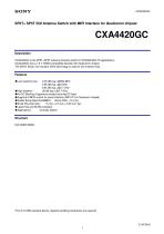
SP5T+ SP5T SOI Antenna Switch with MIPI Interface for Qualcomm chipset CXA4420GC Description CXA4420GC is the SP5T+SP5T antenna diversity switch for WCDMA/3G/LTE applications. CXA4420GC has a 1.8 V CMOS compatible decoder with Qualcomm chipset. The SONY Silicon On Insulator (SOI) technology is used for low insertion loss. Features ◆Low Insertion loss : 0.35 dB (typ.) @800 MHz 0.55 dB (typ.) @2 GHz 0.65 dB (typ.) @2.7 GHz ◆High Isolation : 28 dB (typ.) @2.7 GHz ◆No DC Blocking Capacitors (except sourcing DC bias) ◆Supports CMOS control for serial interface (MIPI I/F for Qualcomm chipset) ◆Solder Bump Bare Die(SBBD): Bump Pitch = 0.4 mm ◆Small Flip-Chip Size : 1.5 mm x 2.3 mm x 0.35 mm Typ. ◆Lead-Free and RoHS compliant ◆Applications: Diversity Switch. Structure SOI CMOS MMIC This IC is ESD sensitive device. Special handling precautions are required
Open the catalog to page 1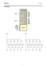
Block Diagram
Open the catalog to page 2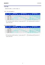
Truth Table USID=0b1010 (SSEL = L) or 0b1011 (SSEL = H) *ANT1 side Series and ANT1 side Shunt ”L” means a switch “OFF”, ANT1 side Series and ANT1 side Shunt ”H” **ANT2 side Series and ANT2 side Shunt ”L” means a switch “OFF”, means a switch “ON” ANT2 side Series and ANT2 side Shunt ”H”
Open the catalog to page 3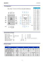
Absolute Maximum Ratings ◆ Supply voltage ◆ Control voltage (MIPI) ◆ Maximum input ◆ Operating temperature DC Bias Condition ( Ta = 25 ℃) Parameter Supply Voltage Interface Supply Voltage SSEL Supply Voltage low SSEL Supply Voltage High Signal level low Signal level high SCLK write Frequency VDD VIO VSSEL_L VSSEL_H Ccl Vch fSCLKw SCLK read Frequency
Open the catalog to page 4
Insertion Loss Inter Modulation Distortion in Rx Band Control Current Supply Current Ivio SDATA,SCLK Active Mode Low Power Mode Active Mode Switching Time From Low Power Mode to Active Mode Electrical Characteristics are measured with all RF ports terminated in 50 Ohms. * 1 freq = 704 MHz to 787 MHz * 2 freq = 824 MHz to 960 MHz * 3 freq = 1710 MHz to 2170 MHz * 4 freq = 2500 MHz to 2690 MHz * 5 Pin = 26 dBm, freq = 824 MHz to 915 MHz * 6 Pin = 26 dBm, freq = 1710 MHz to 1910 MHz * 7 Pin = 26 dBm, freq = 2500 MHz to 2570 MHz * 8 Measured with the recommended circuit * 9-20 Refer to the table...
Open the catalog to page 5
Active path Electrical Characteristics are measured with all RF ports terminated in 50 Ohms. * 21 ANT2 Side is fixed State7 (Isolation) .
Open the catalog to page 7
Active path Electrical Characteristics are measured with all RF ports terminated in 50 Ohms. * 21 ANT2 Side is fixed State7 (Isolation) .
Open the catalog to page 8
Active path Electrical Characteristics are measured with all RF ports terminated in 50 Ohms. * 22 ANT1 Side is fixed State1 (Isolation) .
Open the catalog to page 9
Active path Electrical Characteristics are measured with all RF ports terminated in 50 Ohms. * 22 ANT1 Side is fixed State1 (Isolation) .
Open the catalog to page 10
Electrical Characteristics are measured with all RF ports terminated in 50 Ohms. * 21 ANT2 Side is fixed State7 (Isolation) . * 22 ANT1 Side is fixed State1 (Isolation) .
Open the catalog to page 11
SSEL Specification SSEL (Slave Address) MIPI Specification Supply Voltage Supply current (ACTIVE) *VDD = 2.5 V Supply current Low Power(disable) *VDD = 2.5 V Interface Supply Voltage Supply current (Active) *Vio = 1.8 V Supply current Low Power(disable) *Vio = 1.8 V Signal level high SCLK write Frequency SCLK read Frequency SDATA/SCLK input capacitance Data setup time Data hold time Switching Time* * Switching Time: Timing for switching from an arbitrary state to the next state. ** Turn on time: Time to guarantee RF performance after switch activation.
Open the catalog to page 12
Explanation of Register ・PM_TRIG with three triggers ・Software reset and debug using the RFFE_STATUS register ・Register_0 write ・Full speed write, half speed read ・Extended Read/Write Not Available ・GSID* ・Programmable USID Slave Address : 0b1010 (SSEL = L) or 0b1011 (SSEL = H) Register D0 Register 0 write Command Switch state *See truth table Ant2-RF6toRF10 Switch State Trigger Support. Switch state *See truth table Ant1 side Antenna Switch State Trigger Support. Ant2 side Antenna Switch State Trigger Support. [D7]: SOFTWARE_RESET [D6]: COMMAND_FRAME_PARITY_ERR [D5]: COMMAND_LENGTH_ERR RFFE...
Open the catalog to page 13
- REGISTER_0 Write command Sequence Slave Address Slave Address Wrte Conmand RegEter Address Slave Address Read Gsrrmand Register Address Data frame from ANT Sw itch (Read Half Speed)
Open the catalog to page 14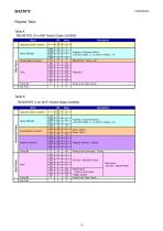
Register Table Table A REGISTER_0 for ANT Switch State (0x0000) Items Sequence Start Condition Data Frame Slave Address Write/Read Command Address of Diversity Switch = 0b1010 (SSEL = L) or 0b1011 (SSEL = H) REGISTER_0 Write : 0b1 Parity bit for Data Frame Table B REGISTER_0 for ANT1 Switch State (0x0000) Items Sequence Start Condition Command Frame Slave Address Write/Read Command Register Address Data Frame Address of Diversity Switch = 0b1010 (SSEL = L) or 0b1011 (SSEL = H) Parity bit for Command Frame [D7:D3] = 0b00000 (Fixed) Initial value : [D7:D0] = 0b0000 0000 Switch State (See the truth...
Open the catalog to page 15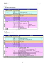
Table C ANT2 Switch State (0x0001) Items Command Frame Slave Address Write/Read Command Register Address Data Frame Sequence Start Condition Address of Diversity Switch = 0b1010 (SSEL = L) or 0b1011 (SSEL = H) Parity bit for Command Frame [D7:D3] = 0b00000 (Fixed) Initial value : [D7:D0] = 0b0000 0000 Switch State (See the truth table) Trigger support Parity bit for Data Frame Table D RFFE_STATUS (0x001A) Items Sequence Start Condition Command Frame Slave Address Write/Read Command Register Address Data Frame Address of Diversity Switch = 0b1010 (SSEL = L) or 0b1011 (SSEL = H) Parity bit for...
Open the catalog to page 16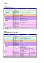
Table E Group Slave ID (0x001B) Items Sequence Start Condition Command Frame Slave Address Write/Read Command Register Address Data Frame Address of Diversity Switch = 0b1010 (SSEL = L) or 0b1011 (SSEL = H) Write : 0b010 Read : 0b011 Parity bit for Command Frame Parity bit for Data Frame Table F Power Mode & Trigger Mode (0x001C) Items Command Frame Slave Address Write/Read Command Register Address Data Frame Sequence Start Condition Address of Diversity Switch = 0b1010 (SSEL = L) or 0b1011 (SSEL = H) Parity bit for Command Frame PWR_MODE[1:0] (R/W) 0b00 : Normal operation (ACTIVE) 0b01: Default...
Open the catalog to page 17All Sony Semiconductors catalogs and technical brochures
 IMX901-AMR
2 Pages
 IMX490
2 Pages
 IMX290NQV
2 Pages
 ISX016
2 Pages
 IMX390CQV
2 Pages
Archived catalogs
 SLD344YT
6 Pages
 SLD432S
5 Pages
 CXA3314ER
16 Pages
 CXB1818Q
17 Pages
 ICX205AK
24 Pages
 CXA2096N
17 Pages
 SLD433S4
5 Pages
 CXA4416GC
21 Pages
 CXA2984GC SP4T ANT SW
11 Pages
 SLD335YT
5 Pages
 CXM3807K
24 Pages
 CXM3648UR
11 Pages
 CXM3645ER
12 Pages
 CXM3642K
29 Pages
 CXM3641ER
22 Pages
 CXM3632ER
22 Pages
 CXM3630UR
15 Pages
 CXM3617ER
23 Pages
 CXM3614ER
14 Pages
 CXM3604UR
14 Pages
 CXM3599UR
15 Pages
 CXM3593UR
11 Pages
 SLD1332V
5 Pages
 CXM3592AUR
15 Pages
 CXM3583AUR
17 Pages
 CXM3582UR
17 Pages
 CXM3580UR
13 Pages
 CXM3580AUR
17 Pages
 CXM3572ER
14 Pages
 CXM3570ER
13 Pages
 CXM3569XR
13 Pages
 ICX418ALB
20 Pages
 CXD4728R
68 Pages
 ICX642BKA
23 Pages
 CXA3791EN
13 Pages
 SLD332F
6 Pages
 CXG1407XR
11 Pages
 IMX291LQR
2 Pages
 IMX252LLR/LQR
2 Pages
 IMX230
2 Pages
 IMX377CQT
5 Pages
 IMX249LLJ/LQJ
2 Pages
 IMX323LQN
2 Pages
 IMX258
2 Pages
 IMX302LQJ
2 Pages
 CXD4017R
34 Pages
 CXA3197R
30 Pages
 IMX222LQJ
2 Pages
 IMX324
2 Pages
 IMX367LLA
2 Pages
 IMX412-AACK
2 Pages
 IMX385LQR
2 Pages
 IMX294CJK
2 Pages
 IMX253LLR/LQR
2 Pages
 IMX273LLR/LQR
2 Pages
 IMX183CLK-J/CQJ-J
2 Pages
 IMX249LLJ/IMX249LQJ
2 Pages
 IMX250LLR/LQR,IMX252LLR/LQR
2 Pages
 B/W Video Camera CCD ICX422AL
17 Pages
 B/W Video Camera CCD ICX279AL*2
18 Pages
 Color Video Camera CCD ICX239AKE
18 Pages
 Color Video Camera CCD ICX418AKL
22 Pages


- Liebherr display
- LCD display panel
- Color display panel
- LED display panel
- RGB display panel
- Compact display panel
- GNSS receiver
- Compact receiver
- Industrial receiver
- OLED display
- High-definition display module
- Laser diode
- Satellite receiver
- Liebherr CMOS image sensor
- Vision sensor
- Communication card
- Full HD display
- Fiber laser diode
- Codec
- Liebherr visible image sensor