- Catalogs
- Sony Semiconductors
- CXA3791EN
- Products
- Catalogs
- News & Trends
- Exhibitions
CXA3791EN
1 /13Pages

CXA3791EN
1 /13Pages
Catalog excerpts
High-speed Buffer Amplifier for CCD Image Sensor The CXA3791 EN is a high-speed buffer amplifier IC. (Applications: CCD image sensor output buffers, Digital still cameras, Camcorders, Other general buffers) (IDRV = 50uA (180kQ when Vcc = 13V), ISF pin connected to GND, during no signal) ♦ High-speed response: 500V/u.s (IDRV = 50uA (180kQ when Vcc = 13V), CL = 20pF) ♦ Internal sink current mode for CCD with open source output (Settable by external resistance RISF) ♦ Enables to set the responsibility by changing the drive current by an external resistor Bipolar silicon monolithic IC Absolute Maximum Ratings ♦ Storage temperature Tstg -65 to+150 °C ♦ Allowable power dissipation PD 0.22 W (when mounted on a two-layer board; 13mm x 13mm, t = 0.63mm) Recommended Operating Conditions Sony reserves the right to change products and specifications without prior notice. This information does not convey any license by any implication or otherwise under any patents or other right. Application circuits shown, if any, are typical examples illustrating the operation of the devices. Sony cannot assume responsibility for any problems arising out of the use of these circuits.
Open the catalog to page 1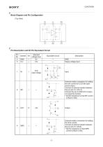
Block Diagram and Pin Configuration (Top View) ISF Pin Description and I/O Pin Equivalent Circuit Pin No. 2 5 Standard voltage level 0V 13V Equivalent circuit — — Description GND. Supply voltage input. External resistor connection for setting the sink current for CCD with open source output. Connect an external resistor between this pin and VCC (Pin 5). Connect this pin to GND (Pin 2) when not using this function. * Set the resistance so that ISF current is 90A or less. External resistor connection for setting the drive current. Connect an external resistor between this pin and VCC (Pin5). *...
Open the catalog to page 2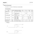
Electrical Characteristics (Ta = 25C, VCC = 13V, RIDRV = 180k, ISF pin: connected to GND) DC Characteristics Item Supply current Measurement conditions Voltage gain RIDRV = 78k RIDRV = 120k RIDRV = 180k RIDRV = 270k Input bias current Sync current Voltage gain
Open the catalog to page 3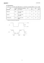
AC Characteristics (Ta = 25C, VCC = 13V, IDRV = 50A (180k when VCC = 13V), ISF pin: connected to GND, RL = 15, CL = 20pF) Item Measurement conditions Rise time Fall time Rise time, fall time and I/O delay time
Open the catalog to page 4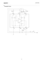
Evaluation Circuit
Open the catalog to page 5
Description of Operation Current Settings 1. Output Drive Current The small signal output impedance of the OUT pin (Pin 3) can be set by connecting the IDRV pin (Pin 4) to VCC through a resistor. The inflow current to the IDRV pin is multiplied by 10 times inside the IC, and flows as the output stage idling current. The IDRV pin has an internal 50k resistor, so the inflow current to the IDRV pin can be calculated as follows. IIDRV = (VCC – VBE 2)/(RIDRV + 50k) = (13 – 1.46)/(180k + 50k) = 50.2A Here, VCC = 13V, VBE = 0.73V (typ.), and RIDRV = 180k. The small signal output impedance at this time...
Open the catalog to page 6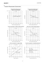
Example of Representative Characteristics (Upper side) I/O voltage range vs. IDRV pin setting resistance (Lower side) I/O voltage range vs. IDRV pin setting resistance IDRV pin setting resistance [kΩ] IDRV pin setting resistance [kΩ] Current consumption vs. IDRV pin setting resistance Sink current vs. ISF pin setting resistance 7.0 IDRV pin setting resistance [kΩ] Current consumption vs. Supply voltage Current consumption vs. Operating temperature 2.0
Open the catalog to page 7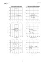
I/O offset voltage vs. Supply voltage I/O offset voltage vs. Operating temperature Input bias current vs. Supply voltage Input bias current vs. Operating temperature Input bias current [µA] Input bias current [µA] Sink current vs. Supply voltage Sink current vs. Operating temperature 3.4
Open the catalog to page 8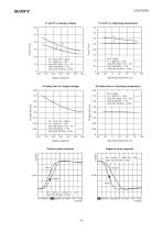
2.0 Ta = 25˚C, Idrv = 50µA, CL = 20pF, RL = 15Ω, Input DC offset = VCC – 5V, Input amplitude = 1.0V, Input rise, fall time = 2.0ns 2.5 2.0 1.5 Idrv = 50µA, CL = 20pF, RL = 15Ω, Input DC offset = VCC – 5V, Input amplitude = 1.0V, Input rise, fall time = 2.0ns I/O delay time vs. Supply voltage I/O delay time vs. Operating temperature 2.00 1.25 1.00 0.75 Ta = 25˚C, Idrv = 50µA, CL = 20pF, RL = 15Ω, Input DC offset = VCC – 5V, Input amplitude = 1.0V, Input rise, fall time = 2.0ns Idrv = 50µA, CL = 20pF, RL = 15Ω, Input DC offset = VCC – 5V, Input amplitude = 1.0V, Input rise, fall time = 2.0ns Positive...
Open the catalog to page 9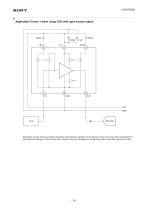
Application Circuit 1 when using CCD with open source output Application circuits shown are typical examples illustrating the operation of the devices. Sony cannot assume responsibility for any problems arising out of the use of these circuits or for any infringement of third party patent and other right due to same.
Open the catalog to page 10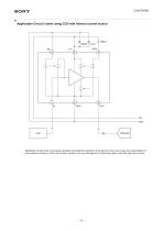
Application Circuit 2 when using CCD with internal current source Application circuits shown are typical examples illustrating the operation of the devices. Sony cannot assume responsibility for any problems arising out of the use of these circuits or for any infringement of third party patent and other right due to same.
Open the catalog to page 11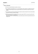
Notes on Operation Provide the widest GND pattern possible on the board. Use a 1000pF (recommended) and a 0.1F (recommended) ceramic capacitors in parallel for the bypass capacitor connected between the power supply and GND, and connect them as close to the IC pins as possible. Load capacitance causes the input/output wiring response to worsen and results in noise. Use the shortest wiring layout possible, and shield it with GND. When the output pin (Pin 3) is shorted to either the power supply or GND, an overcurrent may flow to the output stage elements and damage them. When the input pin (Pin...
Open the catalog to page 12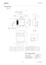
Package Outline Sony Corporation
Open the catalog to page 13All Sony Semiconductors catalogs and technical brochures
 IMX901-AMR
2 Pages
 IMX490
2 Pages
 IMX290NQV
2 Pages
 ISX016
2 Pages
 IMX390CQV
2 Pages
Archived catalogs
 SLD344YT
6 Pages
 SLD432S
5 Pages
 CXA3314ER
16 Pages
 CXB1818Q
17 Pages
 ICX205AK
24 Pages
 CXA2096N
17 Pages
 SLD433S4
5 Pages
 CXA4416GC
21 Pages
 CXA2984GC SP4T ANT SW
11 Pages
 SLD335YT
5 Pages
 CXM3807K
24 Pages
 CXM3648UR
11 Pages
 CXM3645ER
12 Pages
 CXM3642K
29 Pages
 CXM3641ER
22 Pages
 CXM3632ER
22 Pages
 CXM3630UR
15 Pages
 CXM3617ER
23 Pages
 CXM3614ER
14 Pages
 CXM3604UR
14 Pages
 CXM3599UR
15 Pages
 CXM3593UR
11 Pages
 SLD1332V
5 Pages
 CXM3592AUR
15 Pages
 CXM3583AUR
17 Pages
 CXM3582UR
17 Pages
 CXM3580UR
13 Pages
 CXM3580AUR
17 Pages
 CXM3572ER
14 Pages
 CXM3570ER
13 Pages
 CXM3569XR
13 Pages
 ICX418ALB
20 Pages
 CXD4728R
68 Pages
 ICX642BKA
23 Pages
 SLD332F
6 Pages
 CXG1407XR
11 Pages
 IMX291LQR
2 Pages
 IMX252LLR/LQR
2 Pages
 IMX230
2 Pages
 IMX377CQT
5 Pages
 IMX249LLJ/LQJ
2 Pages
 IMX323LQN
2 Pages
 IMX258
2 Pages
 IMX302LQJ
2 Pages
 CXD4017R
34 Pages
 CXA3197R
30 Pages
 IMX222LQJ
2 Pages
 IMX324
2 Pages
 IMX367LLA
2 Pages
 IMX412-AACK
2 Pages
 IMX385LQR
2 Pages
 IMX294CJK
2 Pages
 IMX253LLR/LQR
2 Pages
 IMX273LLR/LQR
2 Pages
 IMX183CLK-J/CQJ-J
2 Pages
 IMX249LLJ/IMX249LQJ
2 Pages
 IMX250LLR/LQR,IMX252LLR/LQR
2 Pages
 B/W Video Camera CCD ICX422AL
17 Pages
 B/W Video Camera CCD ICX279AL*2
18 Pages
 Color Video Camera CCD ICX239AKE
18 Pages
 Color Video Camera CCD ICX418AKL
22 Pages


- Liebherr display
- LCD display panel
- Color display panel
- LED display panel
- RGB display panel
- Compact display panel
- GNSS receiver
- Compact receiver
- Industrial receiver
- OLED display
- High-definition display module
- Laser diode
- Satellite receiver
- Liebherr CMOS image sensor
- Vision sensor
- Communication card
- Full HD display
- Fiber laser diode
- Codec
- Liebherr visible image sensor