- Catalogs
- Sony Semiconductors
- CXA3314ER
- Products
- Catalogs
- News & Trends
- Exhibitions
CXA3314ER
1 /16Pages

CXA3314ER
1 /16Pages
Catalog excerpts
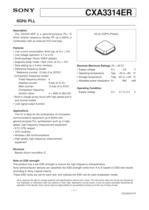
CXA3314ER 6GHz PLL Description The CXA3314ER is a general-purpose PLL IC which directly frequency divides RF up to 6GHz in combination with an external VCO and loop. Features • Low current consumption: 9mA (typ. at VCC = 3V) • Low voltage operation: 2.7 to 3.3V • Small package: 24-pin VQFN (plastic) • Supports sleep mode: 10µA (max. at VCC = 3V) • Data setting by a 3-wire interface • Reference frequency divider Reference counter: 15 bits (3 to 32767) • Comparison frequency divider Fixed frequency division: 4 Swallow counter: 5 bits (0 to 31) Main counter: 13 bits (3 to 8191) Comparison frequency division value: 4 × (992 to 262143) • Built-in charge pump circuit with high-speed pull-in and normal modes • Lock signal output function 24 pin VQFN (Plastic) Absolute Maximum Ratings (Ta = 25°C) • Supply voltage VCC 3.6 V • Operating temperature Topr –30 to +85 °C • Storage temperature Tstg –65 to +150 °C • Allowable power dissipation PD 900 mW Operating Condition Supply voltage VCC 2.7 to 3.3 V Applications This IC is ideal for the synthesizers of microwave communications equipment up to 6GHz and general-purpose PLL synthesizers such as in highspeed, high frequency measurement equipment. • ETC (ITS) related • VCO modules • Wireless LAN communications • High-speed, high frequency measurement equipment Structure Bipolar silicon monolithic IC Note on ESD strength This product has a low ESD strength to ensure the high frequency characteristics. Sony semiconductor devices are classified into ESD strength ranks from A to E based on ESD test results according to Sony original criteria. These ESD ranks are set for each test, and indicate the ESD risk for each breakdown model. Sony reserves the right to change products and specifications without prior notice. This information does not convey any license by any implication or otherwise under any patents or other right. Application circuits shown, if any, are typical examples illustrating the operation of the devices. Sony cannot assume responsibility for any problems arising out of the use of these circuits. –1– E00782E2Z-PS
Open the catalog to page 1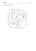
CXA3314ER CPGND DMPSW REXT REFIN VSS VSS Block Diagram and Pin Configuration 18 17 16 15 14 13 CPOUT 19 Test Circuit Lock Detector CP (Fast/Slow) CPVCC 20 Buffer I/2I Reference Counter (15 bits) Intermittent Operation Control Circuit High-speed Pull-in Control SUB 21 12 LKDET 11 CEX 10 DATA 3-wire Control PFD RFINN 22 9 LE 7 TESTDIS Main Counter (13 bits) 2 3 NC 4 5 6 VDD 1 NC Dual Modulus (32, 33) Prescaler VCC GND 24 8 Swallow Counter (5 bits) VDD Fixed Frequency Division (4) Prescaler NC RFINP 23 CLK –2–
Open the catalog to page 2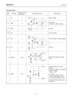
CXA3314ER Pin Description Pin No. Symbol Standard DC voltage [V] Equivalent circuit Description VCC 1 VCC 3 1 21 SUB 0 Power supply. SUB 21 24 GND 0 Substrate. Connect to GND normally. Analog circuit block Ground. 24 GND 2, 3, NC 4 — No connected. 5 5, 6 VDD 3 VDD 6 Power supply for output stage. Digtal circuit block SUB 21 13, 14 VSS 0 Ground. 13 VSS 14 6 100 15 REFIN 1/2VCC VDD 200 100k 15 Reference frequency signal input. 13 21 VSS SUB 6 VDD I 16 REXT 0.15 8.5k 16 13 VSS Internal reference current setting. Connect to GND via a external resistor (1.8kΩ). Icp = I × 6.7 I ≈ IRext Icp: Charge...
Open the catalog to page 3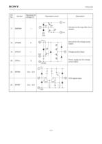
CXA3314ER Pin No. Symbol Standard DC voltage [V] Equivalent circuit Description 6 333 17 DMPSW VDD 666 Connect to the loop filter via a resistor. 17 — 13 VSS 21 SUB CPVCC 18 CPGND 0 19 CPOUT Ground for the charge pump output. 20 — 19 Charge pump output. SUB 21 20 CPVCC 3 Power supply for the charge pump output. 18 CPGND VCC 1 22 RFINN Vcc – 0.9 22 23 2000 23 RFINP 2000 Vcc – 0.9 24 GND –4– VCO signal input.
Open the catalog to page 4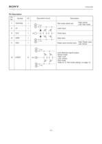
CXA3314ER Pin Description Pin No. 7 Symbol TESTDIS Equivalent circuit I/O I 5 Description Test mode switch pin. VDD High: Active Low: Test mode 6 8 LE I 9 CLK I 10 DATA I Latch input. Clock input. IN Data input. 13 11 CEX I 14 5 VSS Power save function pins. High: Power save Low: Active VDD 6 12 LKDET O Lock detection signal output. •Active mode High: Lock Low: Unlock •Test mode Refer to “2. Test mode setting” on page 12. OUT 12 13 14 VSS –5–
Open the catalog to page 5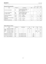
CXA3314ER Electrical Characteristics Item (VCC = 3V, Ta = 25°C) Symbol Conditions Min. Typ. Max. Unit 9 14 mA 10 µA 2 6 GHz Current consumption ICC Current flowing to Pins 1, 6 and 20 during operation (Pin 11 (CEX): 0) Current consumption (in sleep mode) ICC (PS) Current flowing to Pins 1, 6 and 20 in sleep mode (Pin 11 (CEX): High) Operating frequency F-RF V-RF = –10dBm Input level V-RF F-RF = 5.845GHz –12 +10 dBm Reference input operating frequency F-REF V-REF = 0.2Vp-p 10 30 MHz Reference input level V-REF F-REF = 10MHz 0.2 2.0 Vp-p Max. Unit Design Reference Values Item CEX DATA CLK LE Symbol...
Open the catalog to page 6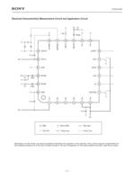
CXA3314ER Electrical Characteristics Measurement Circuit and Application Circuit 51 1.8k 18 17 16 15 14 13 CPGND DMPSW REXT REFIN VSS VSS 1000p 19 CPOUT LKDET 12 0.1µ 20 CPVCC 3V CEX 11 21 SUB DATA 10 22 RFINN 9 LE 8 TESTDIS 7 100p 51 CLK 23 RFINP 51 100p VCC NC NC VDD VDD 1 0.1µ NC 24 GND 2 3 4 5 6 3V 0.1µ 3V SMA Terminal Plane GND Power line 50Ω strip 0.3mm line Application circuits shown are typical examples illustrating the operation of the devices. Sony cannot assume responsibility for any problems arising out of the use of these circuits or for any infringement of third party patent and...
Open the catalog to page 7
CXA3314ER Description of Operation The CXA3314ER can make the following operation settings using the three DT, CK and LE signals. Item Item number Counter frequency division value and pull-in mode settings 1 Reference counter (R counter) frequency division value setting 1-1 Swallow counter and main counter (N counter) frequency division value settings 1-2 Pull-in mode setting 1-3 Initialization 1-4 Test mode 1-5 Test mode setting 2 Standby mode setting 3 1. Counter frequency division value and pull-in mode setting method The CXA3314ER sets data using the three DT, CK and LE signals. At this time,...
Open the catalog to page 8All Sony Semiconductors catalogs and technical brochures
 IMX901-AMR
2 Pages
 IMX490
2 Pages
 IMX290NQV
2 Pages
 ISX016
2 Pages
 IMX390CQV
2 Pages
Archived catalogs
 SLD344YT
6 Pages
 SLD432S
5 Pages
 CXB1818Q
17 Pages
 ICX205AK
24 Pages
 CXA2096N
17 Pages
 SLD433S4
5 Pages
 CXA4416GC
21 Pages
 CXA2984GC SP4T ANT SW
11 Pages
 SLD335YT
5 Pages
 CXM3807K
24 Pages
 CXM3648UR
11 Pages
 CXM3645ER
12 Pages
 CXM3642K
29 Pages
 CXM3641ER
22 Pages
 CXM3632ER
22 Pages
 CXM3630UR
15 Pages
 CXM3617ER
23 Pages
 CXM3614ER
14 Pages
 CXM3604UR
14 Pages
 CXM3599UR
15 Pages
 CXM3593UR
11 Pages
 SLD1332V
5 Pages
 CXM3592AUR
15 Pages
 CXM3583AUR
17 Pages
 CXM3582UR
17 Pages
 CXM3580UR
13 Pages
 CXM3580AUR
17 Pages
 CXM3572ER
14 Pages
 CXM3570ER
13 Pages
 CXM3569XR
13 Pages
 ICX418ALB
20 Pages
 CXD4728R
68 Pages
 ICX642BKA
23 Pages
 CXA3791EN
13 Pages
 SLD332F
6 Pages
 CXG1407XR
11 Pages
 IMX291LQR
2 Pages
 IMX252LLR/LQR
2 Pages
 IMX230
2 Pages
 IMX377CQT
5 Pages
 IMX249LLJ/LQJ
2 Pages
 IMX323LQN
2 Pages
 IMX258
2 Pages
 IMX302LQJ
2 Pages
 CXD4017R
34 Pages
 CXA3197R
30 Pages
 IMX222LQJ
2 Pages
 IMX324
2 Pages
 IMX367LLA
2 Pages
 IMX412-AACK
2 Pages
 IMX385LQR
2 Pages
 IMX294CJK
2 Pages
 IMX253LLR/LQR
2 Pages
 IMX273LLR/LQR
2 Pages
 IMX183CLK-J/CQJ-J
2 Pages
 IMX249LLJ/IMX249LQJ
2 Pages
 IMX250LLR/LQR,IMX252LLR/LQR
2 Pages
 B/W Video Camera CCD ICX422AL
17 Pages
 B/W Video Camera CCD ICX279AL*2
18 Pages
 Color Video Camera CCD ICX239AKE
18 Pages
 Color Video Camera CCD ICX418AKL
22 Pages


- Liebherr display
- LCD display panel
- Color display panel
- LED display panel
- RGB display panel
- Compact display panel
- GNSS receiver
- Compact receiver
- Industrial receiver
- OLED display
- High-definition display module
- Laser diode
- Satellite receiver
- Liebherr CMOS image sensor
- Vision sensor
- Communication card
- Full HD display
- Fiber laser diode
- Codec
- Liebherr visible image sensor