- Catalogs
- Sony Semiconductors
- CXA2973GC SP3T SOI Antenna Switch for Diversity
- Products
- Catalogs
- News & Trends
- Exhibitions
CXA2973GC SP3T SOI Antenna Switch for Diversity
1 /13Pages

CXA2973GC SP3T SOI Antenna Switch for Diversity
1 /13Pages
Catalog excerpts
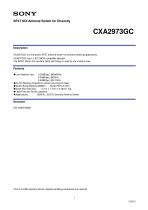
SP3T SOI Antenna Switch for Diversity CXA2973GC Description CXA2973GC is a low power SP3T antenna switch for diversity switching applications. CXA2973GC has a 1.8V CMOS compatible decoder. The SONY Silicon On Insulator (SOI) technology is used for low insertion loss. Features ◆Low Insertion loss : 0.25dB(typ.) @800MHz 0.33dB(typ.) @2GHz 0.40dB(typ.) @2.7GHz ◆No DC Blocking Capacitors (except sourcing DC bias) ◆Solder Bump Bare Die(SBBD) : Bump Pitch=0.4mm ◆Small Flip-Chip Size : 1.1mm x 1.1mm x 0.35mm Typ. ◆Lead-Free and RoHS compliant ◆Applications: GSM Rx, 3G/LTE diversity Antenna Switch Structure SOI CMOS MMIC This IC is ESD sensitive device. Special handling precautions are required
Open the catalog to page 1
Block Diagram Truth Table State State
Open the catalog to page 2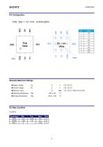
Absolute Maximum Ratings ◆ Supply voltage ◆ Maximum input ◆ Operating temperature
Open the catalog to page 3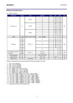
Electrical Characteristics 1 (VDD=2.65V, Ta=25℃) Param eter Insertion Loss All ports in active paths 3fo Inter Modulation Distortion in Rx Band Control Current Supply Current Active Mode freq = 704 to 960 MHz freq = 1710 to 1990 MHz freq = 2110 to 2170 MHz freq = 2500 to 2690 MHz Pin = 26dBm, freq = 824 to 915 MHz Pin = 26dBm, freq = 1710 to 1910 MHz Pin = 26dBm, freq = 1920 to 1980 MHz Pin = 26dBm, freq = 2500 to 2570 MHz Pin on RF: 10dBm, 835MHz, Pin on ANT: -15dBm, 45MHz Pin on RF: 10dBm, 1745MHz, Pin on ANT: -15dBm, 95MHz Pin on RF: 10dBm, 1880MHz, Pin on ANT: -15dBm, 80MHz Pin on RF: 10dBm,...
Open the catalog to page 4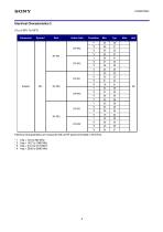
Electrical Characteristics 2 (VDD=2.65V, Ta=25℃) Param eter Active Path Electrical Characteristics are measured with all RF ports terminated in 50 Ohms. *1 *2 *3 *4 freq = 704 to 960 MHz freq = 1427 to 1990 MHz freq = 2110 to 2170 MHz freq = 2500 to 2690 MHz
Open the catalog to page 5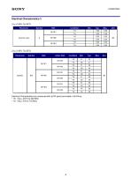
Electrical Characteristics 3 (VDD=2.65V, Ta=25℃) Param eter Insertion Loss Active Path Electrical Characteristics are measured with all RF ports terminated in 50 Ohms. * 18 freq = 207.5 to 222 MHz * 19 freq = 470 to 770 MHz
Open the catalog to page 6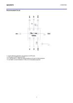
Recommended Circuit *1: No DC blocking capacitors are required on all RF ports. *2: DC levels of all RF ports are GND. *3: L1 (27nH) and C1 (12pF) are recommended on Ant port for ESD protection. *4: C2(100pF) is recommended on VDD pin for Decoupling Capacitor.
Open the catalog to page 7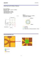
Solder Bump Foot Print (Macro) *Reference Device specification •Device size : 1.1mm × 1.1mm × t 0.350mm •Pin counts : 9Pin •Solder Bump height : 0.150mm •Solder Bump ball size : φ0.2mm •Solder Bump pitch : 0.4mm Detail - A •Land size (Resist Open area) : φ200um •Cu pattern size : (φ300um) : Resist open : Solder print area (Metal mask thickness : 110um) Device Area Via Metal Pattern
Open the catalog to page 8
QM WIDTH EMBOSSED TAPING N0Tf)l. THE R HEASUBEHEHT If I TROUT INDICATION IS ASSDHED TO BE 0. 3n HA!, GEHERAL TOLERANCE: 10, 2 3. THE FEED HOLE ClNllLATlT( PITCH ERROR IS ASSlNEB AT±0. 2n/ I C PITCH. UNIMl
Open the catalog to page 10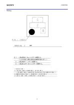
1) TYPE ND. t Ml 1 CHflRftCTERS ) IN SECTION C._ t FOR MORE THAN 2 CHARACTERS FOLLOW RULES FOR ABBREVIATIONS. I 2) MANUFACTURING YEAR ( f CHARACTER } IN SECTION B._ 3) SERIAL CODE ( MAX 3 CHARACTERS ) IN SECTION E.
Open the catalog to page 11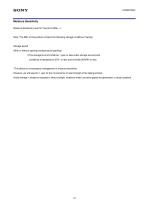
Moisture Sensitivity Moisture Sensitivity Level for this part is MSL = 1 Note: The MSL of this product contains the following storage conditions (Taping). Storage period (With or without opening moisture-proof packing) ⇒The storage time limit shall be 1 year or less under storage environment conditions of temperature 30℃ or less and humidity 85RH or less. *This device is unnecessary management of moisture sensitivity. However, we will assume 1 year for the convenience of seal strength of the taping product. Avoid storage in locations exposed to direct sunlight, locations where corrosive gases...
Open the catalog to page 12
Note Sony reserves the right to change products and specifications without prior notice. This information does not convey any license by any implication or otherwise under any patents or other right. Application circuits shown, if any, are typical examples illustrating the operation of the devices. Sony cannot assume responsibility for any problems arising out of the use of these circuits
Open the catalog to page 13All Sony Semiconductors catalogs and technical brochures
 IMX901-AMR
2 Pages
 IMX490
2 Pages
 IMX290NQV
2 Pages
 ISX016
2 Pages
 IMX390CQV
2 Pages
Archived catalogs
 SLD344YT
6 Pages
 SLD432S
5 Pages
 CXA3314ER
16 Pages
 CXB1818Q
17 Pages
 ICX205AK
24 Pages
 CXA2096N
17 Pages
 SLD433S4
5 Pages
 CXA4416GC
21 Pages
 CXA2984GC SP4T ANT SW
11 Pages
 SLD335YT
5 Pages
 CXM3807K
24 Pages
 CXM3648UR
11 Pages
 CXM3645ER
12 Pages
 CXM3642K
29 Pages
 CXM3641ER
22 Pages
 CXM3632ER
22 Pages
 CXM3630UR
15 Pages
 CXM3617ER
23 Pages
 CXM3614ER
14 Pages
 CXM3604UR
14 Pages
 CXM3599UR
15 Pages
 CXM3593UR
11 Pages
 SLD1332V
5 Pages
 CXM3592AUR
15 Pages
 CXM3583AUR
17 Pages
 CXM3582UR
17 Pages
 CXM3580UR
13 Pages
 CXM3580AUR
17 Pages
 CXM3572ER
14 Pages
 CXM3570ER
13 Pages
 CXM3569XR
13 Pages
 ICX418ALB
20 Pages
 CXD4728R
68 Pages
 ICX642BKA
23 Pages
 CXA3791EN
13 Pages
 SLD332F
6 Pages
 CXG1407XR
11 Pages
 IMX291LQR
2 Pages
 IMX252LLR/LQR
2 Pages
 IMX230
2 Pages
 IMX377CQT
5 Pages
 IMX249LLJ/LQJ
2 Pages
 IMX323LQN
2 Pages
 IMX258
2 Pages
 IMX302LQJ
2 Pages
 CXD4017R
34 Pages
 CXA3197R
30 Pages
 IMX222LQJ
2 Pages
 IMX324
2 Pages
 IMX367LLA
2 Pages
 IMX412-AACK
2 Pages
 IMX385LQR
2 Pages
 IMX294CJK
2 Pages
 IMX253LLR/LQR
2 Pages
 IMX273LLR/LQR
2 Pages
 IMX183CLK-J/CQJ-J
2 Pages
 IMX249LLJ/IMX249LQJ
2 Pages
 IMX250LLR/LQR,IMX252LLR/LQR
2 Pages
 B/W Video Camera CCD ICX422AL
17 Pages
 B/W Video Camera CCD ICX279AL*2
18 Pages
 Color Video Camera CCD ICX239AKE
18 Pages
 Color Video Camera CCD ICX418AKL
22 Pages


- Liebherr display
- LCD display panel
- Color display panel
- LED display panel
- RGB display panel
- Compact display panel
- GNSS receiver
- Compact receiver
- Industrial receiver
- OLED display
- High-definition display module
- Laser diode
- Satellite receiver
- Liebherr CMOS image sensor
- Vision sensor
- Communication card
- Full HD display
- Fiber laser diode
- Codec
- Liebherr visible image sensor