- Catalogs
- Sony Semiconductors
- CXA2096N
- Products
- Catalogs
- News & Trends
- Exhibitions
CXA2096N
1 /17Pages

CXA2096N
1 /17Pages
Catalog excerpts
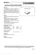
Digital CCD Camera Head Amplifier head amplifier for digital CCD cameras. This IC provides the following functions: correlated double sampling, AGC for the CCD signal, A/D sample and hold, blanking, A/D reference voltage, and an output • High sensitivity made possible by a high-gain AGC • Blanking function provided for the purpose of calibrating the CCD output signal black level • Regulator output pin provided for A/D converter reference voltage * Built-in sample-and-hold circuits for camera signals required by external A/D converters Absolute Maximum Ratings • Operating temperature Topr -20 to +75 °C • Storage temperature Tstg -65 to +150 °C • Allowable power dissipation PD 417 mW Operating Conditions Supply voltage DVC/still cameras for consumer use Bipolar silicon monolithic IC Sony reserves the right to change products and specifications without prior notice. This information does not convey any license by any implication or otherwise under any patents or other right. Application circuits shown, if any, are typical examples illustrating the operation of the devices. Sony cannot assume responsibility for any problems arising out of the use of these circuits.
Open the catalog to page 1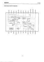
Block Diagram and Pin Configuration
Open the catalog to page 2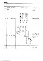
Equivalent circuit Power saving mode. Power supply.
Open the catalog to page 3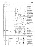
Equivalent circuit normally ground. noise when this pin is noise when this pin is Camera signal preblanking pulse output waveform.
Open the catalog to page 4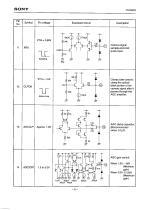
Equivalent circuit Camera signal pulse input. Clamp pulse used to camera signal after it
Open the catalog to page 5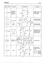
Equivalent circuit camera signal. Preset level sample- and-hold pulse input. Data level sample- and-hold pulse input. Clamp pulse used to Black level DRVOUT output waveform rise time rise time rise time
Open the catalog to page 6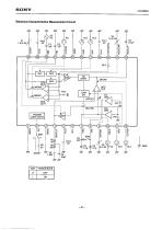
Electrical Characteristics Measurement Circuit
Open the catalog to page 8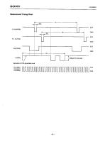
Measurement Timing Chart Equivalent to CCD signal black level Different for each test
Open the catalog to page 9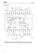
Application Circuit Application circuits shown are typical examples illustrating the operation of the devices. Sony cannot assume responsibility for any problems arising out of the use of these circuits or for any infringement of third party patent and other right due to same.
Open the catalog to page 10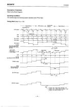
Refer to the Block Diagram. Operating Conditions The camera signal processing system operates when PS is High. Timing Chart (when Vcc = 3V) . during the idle transfer CAMSH output Signal interval Precharge level Idle transfer Signal interval Signal level Basic black Black level transfer interval) DRVOUT output Approx. VRB + 35mV when OFFSET = OV Approx. VRB + 100mV when OFFSET = 1.5V Applox. VRB when OFFSET = 3V
Open the catalog to page 11
The CCD signal from the CCD image sensor is input to PIN and DIN where correlated double sampling (CDS) is performed by SH1, SH2 and SH3. The precharge level of the CCD output signal is sampled, held and output by the SH2 output, and the signal level is sampled, held and output by the SH3 output. SH1 and SH2 are the sample-and-hold circuits for the precharge level; SH3 is the sample-and-hold circuit for the signal level. CDSCLP1 and 2 stabilize the input signal DC level, clamp (CLPDM) the input signal during the idle transfer interval for the purpose of eliminating the AGC input offset, and adjust...
Open the catalog to page 12
DRV drives the external A/D. The current that flows to the last-stage amplifier in DRV is controlled by applying voltage to the 1CONT pin, making it possible to adjust the rise time of the output waveform, which affects the external A/D load capacitance. The variable range is 1.5 to 3V, with 1.5V yielding the maximum and 3V yielding the minimum. The optimum rise time for the external A/D input capacitance can be selected. VRTDRV, VRBDRV: These are the external A/D reference voltage drivers. These circuits are connected to A/D VRT and VRB, supplying 2.35V and 1.35V, respectively, when Vcc is 3V....
Open the catalog to page 13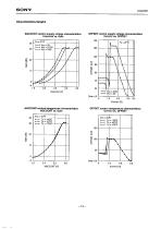
Characteristics Graphs AGCCONT control supply voltage characteristics VAGCCONTVS. Gain OFFSET control supply voltage characteristics AGCCONT control temperature characteristics OFFSET control temperature characteristics VOFFSETVS. OFFSET
Open the catalog to page 14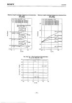
Maximum signal amplitude temperature characteristics Gain temperature characteristics Maximum signal amplitude temperature characteristics
Open the catalog to page 15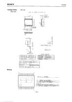
Package Outline I) TVPF NO. 1 MAX 6 CHARACTERS I IN SECTION C. I FOR MORF THAN S CHARACTERS FOLLOW RULES FDR ABSP.EV I AT IOHS
Open the catalog to page 16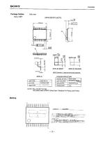
Package Outline NOTE: Dimension does not include mold protrusion. NOTE : PALLADIUM PLATING This product uses S-PdPPF (Sony Spec-Palladium Pre-Plated Lead Frame). ll TYPE NO. ( MAX 6 CHARACTFPS I IN SECTION C. FOR MORE THAN fi CHARACTERS FQIIQ11 HIRES FOR ABBUFVIAT I DNS. 1
Open the catalog to page 17All Sony Semiconductors catalogs and technical brochures
 IMX901-AMR
2 Pages
 IMX490
2 Pages
 IMX290NQV
2 Pages
 ISX016
2 Pages
 IMX390CQV
2 Pages
Archived catalogs
 SLD344YT
6 Pages
 SLD432S
5 Pages
 CXA3314ER
16 Pages
 CXB1818Q
17 Pages
 ICX205AK
24 Pages
 SLD433S4
5 Pages
 CXA4416GC
21 Pages
 CXA2984GC SP4T ANT SW
11 Pages
 SLD335YT
5 Pages
 CXM3807K
24 Pages
 CXM3648UR
11 Pages
 CXM3645ER
12 Pages
 CXM3642K
29 Pages
 CXM3641ER
22 Pages
 CXM3632ER
22 Pages
 CXM3630UR
15 Pages
 CXM3617ER
23 Pages
 CXM3614ER
14 Pages
 CXM3604UR
14 Pages
 CXM3599UR
15 Pages
 CXM3593UR
11 Pages
 SLD1332V
5 Pages
 CXM3592AUR
15 Pages
 CXM3583AUR
17 Pages
 CXM3582UR
17 Pages
 CXM3580UR
13 Pages
 CXM3580AUR
17 Pages
 CXM3572ER
14 Pages
 CXM3570ER
13 Pages
 CXM3569XR
13 Pages
 ICX418ALB
20 Pages
 CXD4728R
68 Pages
 ICX642BKA
23 Pages
 CXA3791EN
13 Pages
 SLD332F
6 Pages
 CXG1407XR
11 Pages
 IMX291LQR
2 Pages
 IMX252LLR/LQR
2 Pages
 IMX230
2 Pages
 IMX377CQT
5 Pages
 IMX249LLJ/LQJ
2 Pages
 IMX323LQN
2 Pages
 IMX258
2 Pages
 IMX302LQJ
2 Pages
 CXD4017R
34 Pages
 CXA3197R
30 Pages
 IMX222LQJ
2 Pages
 IMX324
2 Pages
 IMX367LLA
2 Pages
 IMX412-AACK
2 Pages
 IMX385LQR
2 Pages
 IMX294CJK
2 Pages
 IMX253LLR/LQR
2 Pages
 IMX273LLR/LQR
2 Pages
 IMX183CLK-J/CQJ-J
2 Pages
 IMX249LLJ/IMX249LQJ
2 Pages
 IMX250LLR/LQR,IMX252LLR/LQR
2 Pages
 B/W Video Camera CCD ICX422AL
17 Pages
 B/W Video Camera CCD ICX279AL*2
18 Pages
 Color Video Camera CCD ICX239AKE
18 Pages
 Color Video Camera CCD ICX418AKL
22 Pages


- Liebherr display
- LCD display panel
- Color display panel
- LED display panel
- RGB display panel
- Compact display panel
- GNSS receiver
- Compact receiver
- Industrial receiver
- OLED display
- High-definition display module
- Laser diode
- Satellite receiver
- Liebherr CMOS image sensor
- Vision sensor
- Communication card
- Full HD display
- Fiber laser diode
- Codec
- Liebherr visible image sensor