- Catalogs
- Sony Semiconductors
- Color Video Camera CCD ICX239AKE
- Products
- Catalogs
- News & Trends
- Exhibitions
Color Video Camera CCD ICX239AKE

Color Video Camera CCD ICX239AKE
- High sensitivity and low smear.
- Operates with a horizontal and reset gate drive voltage of 3.3 to 5.0V.
- No voltage adjustment needed for reset gate and substrate bias.
- Low dark current and excellent antiblooming characteristics.
- Continuous variable-speed shutter.
- Recommended exit pupil distance: –10mm to –∞.
- Interline CCD with a diagonal size of 3mm (Type 1/6).
- Effective pixels: 752 (H) × 582 (V), approximately 440K pixels.
- Total pixels: 795 (H) × 596 (V), approximately 470K pixels.
- Chip size: 3.30mm (H) × 2.95mm (V).
- Unit cell size: 3.275µm (H) × 3.150µm (V).
- Optical black: Horizontal direction: Front 3 pixels, rear 40 pixels; Vertical direction: Front 12 pixels, rear 2 pixels.
- Substrate material: Silicon.
- Suitable for general electronic equipment but not for critical applications posing life-threatening risks or significant property damage.
- Not for use in weapon or military equipment.
- Supply voltage: 14.55 to 15.45V.
- Operating temperature: -10 to +60°C.
- Storage temperature: -30 to +80°C.
- Clock voltage and bias conditions specified for optimal performance.
- Sensitivity Ratio: Adjust luminous intensity for a Y signal output of 200mV and measure Mg, G, Ye, and Cy signal outputs.
- Saturation Signal: Increase luminous intensity to 10 times the standard and measure the minimum Y signal value.
- Smear: Adjust luminous intensity to 500 times the standard and measure the maximum Y signal output.
- Video Signal Shading: Measure Y signal maximum and minimum values and calculate SHy.
- Uniformity Between Video Signal Channels: Measure maximum and minimum values of R-Y and B-Y channels and calculate ΔSr and ΔSb.
- Dark Signal: Measure Y signal output at 60°C in a light-obstructed state.
- Flicker: Measure signal level differences between fields for Y, Cr, and Cb signals and calculate Fy, Fcr, and Fcb.
- Line Crawls: Measure differences between Y signal lines for various filters and calculate Lci.
- Static Charge Prevention: Use non-chargeable materials, earth bands, and conductive mats. Ionized air is recommended for discharge.
- Soldering: Avoid exceeding 80°C on ceramic surfaces, use a 30W soldering iron, and avoid solder suction equipment.
- Dust and Dirt Protection: Perform operations in a clean room, avoid touching glass surfaces, and clean with ethyl alcohol if necessary.
- Installation: Use elastic loads or adhesives for installation, and avoid using metal that may generate dust.
- Other Considerations: Avoid exposure to strong light and high temperatures or humidity to prevent damage and discoloration.
Catalog excerpts
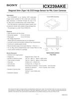
Description The ICX239AKE is an interline CCD solid-stateimage sensor suitable for PAL small color cameras. High resolution is achieved through the use of Ye, Cy, Mg, and G complementary color mosaic filters.This chip features a field period readout system andan electronic shutter with variable charge-storage time.The package is a small 12-pin SON(LCC). 12 pin SON (Ceramic) Features High sensitivity and low smear ? Horizontal register:3.3 to 5.0V drive ? Reset gate:3.3 to 5.0V drive ? No voltage adjustment(Reset gate and substrate bias are not adjusted.) ? Low dark current and excellent antiblooming characteristics ? Continuous variable-speed shutter > Pin 1V340 212 ? Recommended range of exit pupil distance: Ֆ10mm to ֢Ȟ ? Ye, Cy, Mg, and G complementary color mosaic filters on chip ? 12-pin ceramic SON(LCC) package Device Structure? Interline CCD image sensor ? Image size:Diagonal 3mm (Type 1/6) > Pin 7 H ? Number of effective pixels:752 (H) 582 (V) approx. 440K pixels ? Total number of pixels:795 (H) ח 596 (V) approx. 470K pixels Optical black position(Top View) ? Chip size:3.30mm (H) 2.95mm (V) ? Unit cell size:3.275m (H) 3.150m (V) ? Optical black:Horizontal (H) direction:Front 3 pixels, rear 40 pixelsVertical (V) direction:Front 12 pixels, rear 2 pixels ? Number of dummy bits:Horizontal 22Vertical 1 (even fields only) ? Substrate material:Silicon 1֖ > E98X20C3ZSony reserves the right to change products and specifications without prior notice. This information does not convey any license byany implication or otherwise under any patents or other right. Application circuits shown, if any, are typical examples illustrating theoperation of the devices. Sony cannot assume responsibility for any problems arising out of the use of these circuits. size="-1">
Open the catalog to page 1
ICX239AKE USE RESTRICTION NOTICE (December 1, 2003 ver.) Use Restrictions ? The Products are intended for incorporation into such general electronic equipment as office products,communication products, measurement products, and home electronics products in accordance with the terms and conditions set forth in this specifications book and otherwise notified by Sony from time to time. This USE RESTRICTION NOTICE ("Notice") is for customers who are considering or currently using the CCDproducts ("Products") set forth in this specifications book. Sony Corporation ("Sony") may, at any time, modify...
Open the catalog to page 2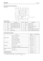
ICX239AKE Block Diagram and Pin Configuration (Top View) > 3 2 4 1 φ OUT φ φ φ V V GND V V V 6 5 4 3 2 1 Pin Description > CyCyMgGCyMg YeYeGMgYeG CyCyMgGCyMg YeYeGMgYeG Symbol φ > Vertical register Note)Note) : Photo sensor Horizontal register 7 8 9 10 11 12 2 1 L φ φ V DD RG H H V SUB φ Absolute Maximum Ratings Pin No.12 3 4 5 6V > 4 Vertical register transfer clock Vertical register transfer clock Vertical register transfer clock Vertical register transfer clock GND Signal output78 910 11 12V > DD Supply voltageSubstrate clock Protective transistor bias Reset gate clock Horizontal register...
Open the catalog to page 3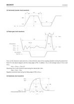
V > RGH Point AtwlV RG waveformV φ > RG V > RGLH V > RGL RGLL V > RGLm H φ > 1 waveform twhtrtf V φ > H /2 [V] > 90%100% 10%0%V ֏ M V Ə > SUB Ə M2 > SUB (A bias generated within the CCD) trtwhtf >
Open the catalog to page 7
ICX239AKE Definition of standard imaging conditions 1)Standard imaging condition I :Use a pattern box (luminance 706cd/m > 2 , color temperature of 3200K halogen source) as a subject. (Patternfor evaluation is not applicable.) Use a testing standard lens with CM500S (t = 1.0mm)as an IR cut filter andimage at F5.6. The luminous intensity to the sensor receiving surface at this point is defined as the standard sensitivity testing luminous intensity.2)Standard imaging condition II :Image a light source (color temperature of 3200K) with a uniformity of brightness within 2% at all angles. Use a testing...
Open the catalog to page 11
ICX239AKE 6.Uniformity between video signal channelsSet to standard imaging condition II . Adjust the luminous intensity so that the average value of the Y signaloutput is 200mV, and then measure the maximum (Crmax, Cbmax [mV]) and minimum (Crmin, Cbmin [mV]) values of the R Y and B ֖ Y channels of the chroma signal and substitute the values into the following formula. ∆ Sr = | (Crmax Crmin)/200 | ֗ 100 [%] ∆ Sb = | (Cbmax Cbmin)/200 | ֗ 100 [%]7.Dark signalMeasure the average value of the Y signal output (Ydt [mV]) with the device ambient temperature 60C and the device in the light-obstructed...
Open the catalog to page 12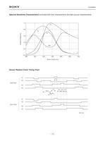
1.00.80.60.40.20.0 YeCyGMg > Relative Response 700650600550500450400Wave Length [nm] > 2.62.62.62.61.533.6 Odd Field Even Field V1V2V3V4V1V2V3V4 0.2 Unit: s >
Open the catalog to page 14
ICX239AKE Notes on Handling 1)Static charge preventionCCD image sensors are easily damaged by static discharge. Before handling be sure to take the following protective measures. a)Either handle bare handed or use non-chargeable gloves, clothes or material. Also use conductive shoes.b)When handling directly use an earth band. c)Install a conductive mat on the floor or working table to prevent the generation of static electricity. d)Ionized air is recommended for discharge when handling CCD image sensor. e)For the shipment of mounted substrates, use boxes treated for the prevention of static charges.2)Solderinga)Make...
Open the catalog to page 17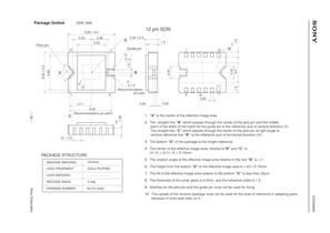
3.53 3.36 2.30 ѱ 0.3 A Pilot pin > 5.52 1.8 11 - 1.0 Guide pin > + 0.13 0 1.0 0.2 ֱ 90˚ 2.43 2.43 6.82 BD C 4.0 8.00 2 - HV φ 1.0 (Recommendatory pin size) 1.5 16 712 16 712 (Recommendatory pin pitch) 12- 0.60 4.11 0.50 0.40 18֖ 8.22 1. AӔ is the center of the effective image area. > 12 - 1.35 2 . The straight line CӔ BӔ which passes through the center of the pilot pin at right angle to vertical reference line which passes through the center of the pilot pin and the middle point of the width of the notch for the guide pin is the reference axis of vertical direction (V). The straight line BӔ is...
Open the catalog to page 18All Sony Semiconductors catalogs and technical brochures
 IMX901-AMR
2 Pages
 IMX490
2 Pages
 IMX290NQV
2 Pages
 ISX016
2 Pages
 IMX390CQV
2 Pages
Archived catalogs
 SLD344YT
6 Pages
 SLD432S
5 Pages
 CXA3314ER
16 Pages
 CXB1818Q
17 Pages
 ICX205AK
24 Pages
 CXA2096N
17 Pages
 SLD433S4
5 Pages
 CXA4416GC
21 Pages
 CXA2984GC SP4T ANT SW
11 Pages
 SLD335YT
5 Pages
 CXM3807K
24 Pages
 CXM3648UR
11 Pages
 CXM3645ER
12 Pages
 CXM3642K
29 Pages
 CXM3641ER
22 Pages
 CXM3632ER
22 Pages
 CXM3630UR
15 Pages
 CXM3617ER
23 Pages
 CXM3614ER
14 Pages
 CXM3604UR
14 Pages
 CXM3599UR
15 Pages
 CXM3593UR
11 Pages
 SLD1332V
5 Pages
 CXM3592AUR
15 Pages
 CXM3583AUR
17 Pages
 CXM3582UR
17 Pages
 CXM3580UR
13 Pages
 CXM3580AUR
17 Pages
 CXM3572ER
14 Pages
 CXM3570ER
13 Pages
 CXM3569XR
13 Pages
 ICX418ALB
20 Pages
 CXD4728R
68 Pages
 ICX642BKA
23 Pages
 CXA3791EN
13 Pages
 SLD332F
6 Pages
 CXG1407XR
11 Pages
 IMX291LQR
2 Pages
 IMX252LLR/LQR
2 Pages
 IMX230
2 Pages
 IMX377CQT
5 Pages
 IMX249LLJ/LQJ
2 Pages
 IMX323LQN
2 Pages
 IMX258
2 Pages
 IMX302LQJ
2 Pages
 CXD4017R
34 Pages
 CXA3197R
30 Pages
 IMX222LQJ
2 Pages
 IMX324
2 Pages
 IMX367LLA
2 Pages
 IMX412-AACK
2 Pages
 IMX385LQR
2 Pages
 IMX294CJK
2 Pages
 IMX253LLR/LQR
2 Pages
 IMX273LLR/LQR
2 Pages
 IMX183CLK-J/CQJ-J
2 Pages
 IMX249LLJ/IMX249LQJ
2 Pages
 IMX250LLR/LQR,IMX252LLR/LQR
2 Pages
 B/W Video Camera CCD ICX422AL
17 Pages
 B/W Video Camera CCD ICX279AL*2
18 Pages
 Color Video Camera CCD ICX418AKL
22 Pages


- Liebherr display
- LCD display panel
- Color display panel
- LED display panel
- RGB display panel
- Compact display panel
- GNSS receiver
- Compact receiver
- Industrial receiver
- OLED display
- High-definition display module
- Laser diode
- Satellite receiver
- Liebherr CMOS image sensor
- Vision sensor
- Communication card
- Full HD display
- Fiber laser diode
- Codec
- Liebherr visible image sensor