- Catalogs
- Sony Semiconductors
- B/W Video Camera CCD ICX279AL*2
- Products
- Catalogs
- News & Trends
- Exhibitions
B/W Video Camera CCD ICX279AL*2

B/W Video Camera CCD ICX279AL*2
- Enhanced sensitivity in the near-infrared region (+5dB at λ = 945nm) and overall high sensitivity (+6dB without IR cut filter).
- Low smear (-20dB) and high dynamic range (+2dB) compared to the ICX209AL.
- Horizontal and reset gate drive voltage: 3.3 to 5V, with no voltage adjustment needed.
- High resolution, low smear, and excellent antiblooming characteristics.
- Continuous variable-speed shutter and recommended exit pupil distance: -20 to -100mm.
- Image size: Diagonal 4.5mm (Type 1/4).
- Effective pixels: 752 (H) × 582 (V), approximately 440K pixels.
- Total pixels: 795 (H) × 596 (V), approximately 470K pixels.
- Chip size: 4.43mm (H) × 3.69mm (V).
- Unit cell size: 4.85µm (H) × 4.65µm (V).
- Substrate material: Silicon.
- Intended for general electronic equipment, not for critical applications posing life-threatening risks or military use.
- Sony disclaims liability for misuse or deviation from specified use.
- Absolute maximum ratings and clock voltage conditions are specified for various components, including vertical and horizontal transfer clocks, reset gate, and substrate clocks.
- Image sensor characteristics include sensitivity, saturation signal, smear, video signal shading, dark signal, and flicker, with specific measurement methods outlined.
- Signal Height (SH): Calculated using the formula SH = (Vmax – Vmin)/200 × 100 [%], where Vmax and Vmin are the maximum and minimum signal output values in mV.
- Dark Signal: Measure the average signal output (Vdt) at 60°C with the device in a light-obstructed state.
- Dark Signal Shading: Calculate ∆Vdt = Vdmax – Vdmin, where Vdmax and Vdmin are the maximum and minimum dark signal output values.
- Flicker: Under standard imaging condition III, adjust luminous intensity for a 200mV average signal output and calculate F = (∆Vf/200) × 100 [%], where ∆Vf is the difference in signal level between fields.
- Lag: Measure residual signal (Vlag) after strobe light adjustment and calculate Lag = (Vlag/200) × 100 [%].
- Static Charge Prevention: Use non-chargeable materials, conductive shoes, and ionized air to prevent static discharge damage.
- Soldering: Limit package temperature to 80°C, use a 30W soldering iron, and avoid solder suction equipment.
- Dust and Dirt Protection: Perform assembly in a clean room, avoid touching glass surfaces, and clean with ethyl alcohol if necessary.
- Installation: Apply static loads within specified limits, use elastic loads or adhesives for installation, and avoid applying loads to the glass portion.
- Other Considerations: Avoid exposure to strong light and high temperatures, and note that the sensor has sensitivity in the near-infrared area.
- Package Outline: Dimensions and tolerances are specified, with a focus on maintaining the integrity of the effective image area.
- Material and Treatment: The package is made of plastic with gold plating, and the lead material is 42 alloy.
- Defects and Tolerances: Specifications for cover glass defects and package structure are provided to ensure quality and performance.
Catalog excerpts
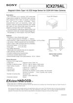
Description The ICX279AL is an interline CCD solid-stateimage sensor suitable for CCIR B/W video cameras with a diagonal 4.5mm (Type 1/4) system. Comparedwith the current product ICX209AL, basiccharacteristics such as sensitivity, smear and dynamic range are improved drastically from visiblelight region to near infrared light region through theadoption of EXview HAD CCD 14 pin DIP (Plastic) > TM technology.This chip features a field period readout system andan electronic shutter with variable charge-storage time.The package is a 10mm-square 14-pin DIP (Plastic). Features Sensitivity in near infrared light region(+5dB compared with the ICX209AL, Վ = 945nm) > Pin 1 ? High sensitivity (+6dB compared with the ICX209AL, no IR cut filter) > 2 ? Low smear (ۖ20dB compared with the ICX209AL) ? High D range (+2dB compared with the ICX209AL) ? Horizontal register:3.3 to 5V drive ? Reset gate:3.3 to 5V drive ? No voltage adjustment(Reset gate and substrate bias are not adjusted.) > 12VH 403 ? High resolution and low smear > Pin 8 ? Excellent antiblooming characteristics ? Continuous variable-speed shutter Optical black position(Top View) ? Recommended range of exit pupil distance: 20 to ֖100mm Device Structure? Interline CCD image sensor ? Image size:Diagonal 4.5mm (Type 1/4) ? Number of effective pixels:752 (H) 582 (V) approx. 440K pixels ? Total number of pixels:795 (H) ח 596 (V) approx. 470K pixels ? Chip size:4.43mm (H) 3.69mm (V) ? Unit cell size:4.85m (H) 4.65m (V) ? Optical black:Horizontal (H) direction: Front 3 pixels, rear 40 pixelsVertical (V) direction: Front 12 pixels, rear 2 pixels ? Number of dummy bits:Horizontal 22Vertical 1 (even fields only) ? Substrate material:Silicon > ∗ EXview HAD CCD is a trademark of Sony Corporation.EXview HAD CCD is a CCD that drastically improves light efficiency by including near infrared light region as a basic structure ofHAD (Hole-Accumulation-Diode) sensor. 1 ֖ > E00Z52A3ZSony reserves the right to change products and specifications without prior notice. This information does not convey any license byany implication or otherwise under any patents or other right. Application circuits shown, if any, are typical examples illustrating theoperation of the devices. Sony cannot assume responsibility for any problems arising out of the use of these circuits. size="-1">
Open the catalog to page 1
ICX279AL USE RESTRICTION NOTICE (December 1, 2003 ver.) This USE RESTRICTION NOTICE ("Notice") is for customers who are considering or currently using the CCDproducts ("Products") set forth in this specifications book. Sony Corporation ("Sony") may, at any time, modify this Notice which will be available to you in the latest specifications book for the Products. You should abide bythe latest version of this Notice. If a Sony subsidiary or distributor has its own use restriction notice on theProducts, such a use restriction notice will additionally apply between you and the subsidiary or distributor....
Open the catalog to page 2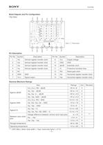
∗ > ICX279AL Block Diagram and Pin Configuration (Top View) > 1 2 3 4 φ φ φ OUT φ V GNDV V V V NC 7 6 5 4 3 2 1 φ > Vertical Register Note)Note) : Photo sensor Horizontal Register 8 9 10 11 12 13 14 L 1 2 φ φ DD RGH H V SUBV GND φ Pin Description Absolute Maximum Ratings Pin No.SymbolDescriptionPin No.SymbolDescription1 2 3 4 5 6 7 V > 4 Vertical register transfer clock Vertical register transfer clock Vertical register transfer clock Vertical register transfer clockGNDSignal output 8910 11 12 13 14 V > DD Supply voltageGND Substrate clock Protective transistor bias Reset gate clock Horizontal...
Open the catalog to page 3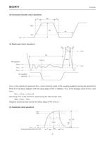
ICX279AL (3) Horizontal transfer clock waveform (4) Reset gate clock waveform > trtwhtf90%10%twlV φ H V HL V RGH Point AtwlV φ RG RG waveformV V RGLH V RGL RGLL V RGLm H φ 1 waveform twhtrtf V φ H /2 [V] V > RGLH is the maximum value and V > RGLL is the minimum value of the coupling waveform during the period fromPoint A in the above diagram until the rising edge of RG. In addition, V > RGL is the average value of V > RGLH andV > RGLL .V > RGL = (V > RGLH + V > RGLL )/2Assuming V > RGH is the minimum value during the interval twh, then:V φ > RG = V > RGH V > RGL Negative overshoot level during...
Open the catalog to page 7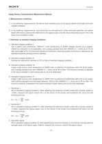
ICX279AL Image Sensor Characteristics Measurement Method Measurement conditions 1)In the following measurements, the device drive conditions are at the typical values of the bias and clockvoltage conditions.2)In the following measurements, spot blemishes are excluded and, unless otherwise specified, the opticalblack (OB) level is used as the reference for the signal output, and the value measured at point [ ∗ A] in thedrive circuit example is used. Definition of standard imaging conditions 1)Standard imaging condition I :Use a pattern box (luminance: 706cd/m > 2 , color temperature of 3200K halogen...
Open the catalog to page 10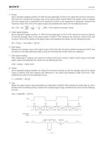
ICX279AL 4.SmearSet to standard imaging condition III . With the lens diaphragm at F5.6 to F8, adjust the luminous intensity to500 times the intensity with average value of the signal output, 200mV. When the readout clock is stoppedand the charge drain is executed by the electronic shutter at the respective H blankings, measure the maximum value YSm [mV] of the signal output and substitute the value into the following formula.Sm = 20 log ח [dB] (1/10V method conversion value)5.Video signal shadingSet to standard imaging condition VSm200 1500 110 IV . With the lens diaphragm at F5.6 to F8, adjust...
Open the catalog to page 11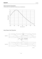
Relative Response 2.62.62.62.633.6 1.5 0.2 Unit: s Odd Field Even Field V1V2V3V4V1V2V3V4 >
Open the catalog to page 13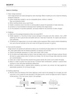
50N50N 1.2Nm Plastic packageCover glass Compressive strength Torsional strength >
Open the catalog to page 16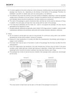
ICX279AL b)If a load is applied to the entire surface by a hard component, bending stress may be generated and thepackage may fracture, etc., depending on the flatness of the bottom of the package. Therefore, for installation, use either an elastic load, such as a spring plate, or an adhesive.c)The adhesive may cause the marking on the rear surface to disappear, especially in case the regulatedvoltage value is indicated on the rear surface. Therefore, the adhesive should not be applied to this area, and indicated values should be transferred to the other locations as a precaution.d)The notch...
Open the catalog to page 17All Sony Semiconductors catalogs and technical brochures
 IMX901-AMR
2 Pages
 IMX490
2 Pages
 IMX290NQV
2 Pages
 ISX016
2 Pages
 IMX390CQV
2 Pages
Archived catalogs
 SLD344YT
6 Pages
 SLD432S
5 Pages
 CXA3314ER
16 Pages
 CXB1818Q
17 Pages
 ICX205AK
24 Pages
 CXA2096N
17 Pages
 SLD433S4
5 Pages
 CXA4416GC
21 Pages
 CXA2984GC SP4T ANT SW
11 Pages
 SLD335YT
5 Pages
 CXM3807K
24 Pages
 CXM3648UR
11 Pages
 CXM3645ER
12 Pages
 CXM3642K
29 Pages
 CXM3641ER
22 Pages
 CXM3632ER
22 Pages
 CXM3630UR
15 Pages
 CXM3617ER
23 Pages
 CXM3614ER
14 Pages
 CXM3604UR
14 Pages
 CXM3599UR
15 Pages
 CXM3593UR
11 Pages
 SLD1332V
5 Pages
 CXM3592AUR
15 Pages
 CXM3583AUR
17 Pages
 CXM3582UR
17 Pages
 CXM3580UR
13 Pages
 CXM3580AUR
17 Pages
 CXM3572ER
14 Pages
 CXM3570ER
13 Pages
 CXM3569XR
13 Pages
 ICX418ALB
20 Pages
 CXD4728R
68 Pages
 ICX642BKA
23 Pages
 CXA3791EN
13 Pages
 SLD332F
6 Pages
 CXG1407XR
11 Pages
 IMX291LQR
2 Pages
 IMX252LLR/LQR
2 Pages
 IMX230
2 Pages
 IMX377CQT
5 Pages
 IMX249LLJ/LQJ
2 Pages
 IMX323LQN
2 Pages
 IMX258
2 Pages
 IMX302LQJ
2 Pages
 CXD4017R
34 Pages
 CXA3197R
30 Pages
 IMX222LQJ
2 Pages
 IMX324
2 Pages
 IMX367LLA
2 Pages
 IMX412-AACK
2 Pages
 IMX385LQR
2 Pages
 IMX294CJK
2 Pages
 IMX253LLR/LQR
2 Pages
 IMX273LLR/LQR
2 Pages
 IMX183CLK-J/CQJ-J
2 Pages
 IMX249LLJ/IMX249LQJ
2 Pages
 IMX250LLR/LQR,IMX252LLR/LQR
2 Pages
 B/W Video Camera CCD ICX422AL
17 Pages
 Color Video Camera CCD ICX239AKE
18 Pages
 Color Video Camera CCD ICX418AKL
22 Pages


- Liebherr display
- LCD display panel
- Color display panel
- LED display panel
- RGB display panel
- Compact display panel
- GNSS receiver
- Compact receiver
- Industrial receiver
- OLED display
- High-definition display module
- Laser diode
- Satellite receiver
- Liebherr CMOS image sensor
- Vision sensor
- Communication card
- Full HD display
- Fiber laser diode
- Codec
- Liebherr visible image sensor