

DDR4 SDRAM Device Operation

DDR4 SDRAM Device Operation
This document provides comprehensive technical information on DDR4 SDRAM, focusing on initialization, reset procedures, and mode register settings. It outlines the necessary steps for powering up and initializing the device to ensure proper operation.
- Simplified State Diagram: An overview of DDR4 SDRAM states and transitions.
- Basic Functionality: Describes fundamental operations, emphasizing high-speed operation and burst-oriented read/write operations.
- RESET and Initialization Procedure: Details the power-up sequence, including VDD slew rate and reset initialization with stable power.
- Register Definition: Covers programming mode registers and their functions.
- Command Truth Table: Lists commands and their corresponding operations.
- Burst Length, Type, and Order: Discusses burst operations, including BL8 burst order with CRC enabled.
- DLL-off Mode & DLL Switching Procedure: Explains procedures for switching DLL modes.
- Input Clock Frequency Change: Guidelines for changing input clock frequency.
- Write Leveling: Describes settings and procedures for write leveling.
- Temperature Controlled Refresh Modes: Details normal and extended temperature modes and their parameters.
- Fine Granularity Refresh Mode: Discusses mode register settings and refresh rate changes.
- Multi Purpose Register: Covers DQ training and MPR read/write operations.
- Data Mask, Data Bus Inversion, and TDQS: Explains functionalities and applications.
- ZQ Calibration Commands: Describes the ZQ calibration process.
- DQ Vref Training: Provides example scripts for VREFDQ calibration.
- Per DRAM Addressability: Discusses addressability features.
- CAL Mode: Details command address latency and related timings.
- CRC: Covers CRC polynomial, data bit mapping, and error handling.
- Command Address Parity: Describes parity error logging and readout.
- Control Gear Down Mode: Explains the mode and its implications.
- DDR4 Key Core Timing: Lists critical timing parameters.
- Programmable Preamble: Discusses write and read preamble settings.
- Postamble: Details read and write postamble operations.
- ACTIVATE Command: Describes the command and its function.
- Precharge Command: Explains the precharge operation.
- Read Operation: Covers read timing definitions and burst operations.
- Write Operation: Discusses write timing parameters and burst operations.
- Refresh Command: Details the refresh operation and its parameters.
- Self Refresh Operation: Describes low power auto self-refresh and exit procedures.
- Power Down Mode: Explains power-down entry, exit, and clarifications.
- Maximum Power Saving Mode: Discusses mode entry and CKE transitions.
Outlines procedures for exiting various modes, including Maximum Power Saving Mode, and details timing parameters associated with these transitions.
Introduces the Connectivity Test Mode, detailing pin mapping, logic equations for different device configurations, and input level requirements.
Describes both hard and soft post-package repair processes, including timing diagrams and programming support for hPPR and sPPR.
Discusses various ODT modes, including synchronous, dynamic, and asynchronous modes, covering ODT latency, timing parameters, and the impact of ODT during reads.
Provides absolute maximum ratings, AC & DC operating conditions, and input measurement levels, including detailed specifications for differential and single-ended signals, overshoot and undershoot specifications, and slew rate definitions.
Covers the DC electrical characteristics of output drivers, including specific characteristics for the Connectivity Test Mode, and details on single-ended and differential output levels.
Includes a speed bin table and outlines IDD and IDDQ specification parameters and test conditions.
Outlines various timing parameters and specifications for DDR4 memory, focusing on DQS timing in relation to the clock signal, with key parameters including tDQSCK with DLL On and Off, and their sensitivity to voltage and temperature.
Proper initialization and configuration of DDR4 SDRAM are essential for its reliable operation. The document provides comprehensive guidelines and timing requirements to ensure that the device is set up correctly.
Catalog excerpts
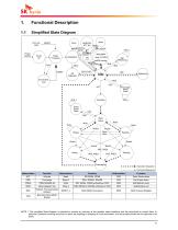
Functional Description Simplified State Diagram from any state Power Applied MPSM IVREFDQ, RTT,Etc MRS SRX w/NOP MRS SRX w/ NOP MRS MRS,MPR, w/ Q=Low Initialization PDA Write Leveling Reset Procedure ZQCL RESET Connectivity Test Precharge Power Down CKE_L Active Power Down Read WriteA ReadA Read Write WriteA ReadA Automatic Sequence Command Sequence Enter Power-down Exit Power-down Self-Refresh entry Self-Refresh exit Refresh, Fine granularity Refresh Start RESET procedure Multi Purpose Register Boundary Scan Mode Enable NOTE 1 This simplified State Diagram is intended to provide an overview...
Open the catalog to page 6
Basic Functionality The DDR4 SDRAM is a high-speed dynamic random-access memory internally configured as sixteen-banks, 4 bank group with 4 banks for each bank group for x4/x8 and eight-banks, 2 bank group with 4 banks for each bankgroup for x16 DRAM. The DDR4 SDRAM uses a 8n prefetch architecture to achieve high-speed operation. The 8n prefetch architecture is combined with an interface designed to transfer two data words per clock cycle at the I/O pins. A single read or write operation for the DDR4 SDRAM consists of a single 8n-bit wide, four clock data transfer at the internal DRAM core and...
Open the catalog to page 7
RESET and Initialization Procedure For power-up and reset initialization, in order to prevent DRAM from functioning improperly default values for the following MR settings need to be defined. Gear down mode (MR3 A[3]) : 0 = 1/2 Rate Per DRAM Addressability (MR3 A[4]) : 0 = Disable Max Power Saving Mode (MR4 A[1]) : 0 = Disable CS to Command/Address Latency (MR4 A[8:6]) : 000 = Disable CA Parity Latency Mode (MR5 A[2:0]) : 000 = Disable Hard Post Package Repair mode (MR4 A[13]) : 0 = Disable Soft Post Package Repair mode (MR4 A[5]) : 0 = Disable Power-up Initialization Sequence The following sequence...
Open the catalog to page 8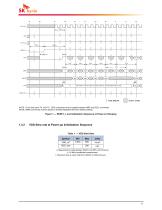
Static LOW in case RTT_Nom is eanbled at time Tg, otherwise static HIGH or LOW TIME BREAK DON’T CARE NOTE 1 From time point ‘Td’ until ‘Tk’, DES commands must be applied between MRS and ZQCL commands. NOTE 2 MRS Commands must be issued to all Mode Registers that have defined settings. Figure 1 — RESET_n and Initialization Sequence at Power-on Ramping VDD Slew rate at Power-up Initialization Sequence Table 1 — VDD Slew Rate Symbol a. Measurement made between 300mV and 80% Vdd minimum. b. 20 MHz bandlimited measurement. c. Maximum time to ramp VDD from 300mV to VDD
Open the catalog to page 9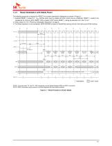
Reset Initialization with Stable Power The following sequence is required for RESET at no power interruption initialization as shown in Figure 2. 1. Asserted RESET_n below 0.2 * VDD anytime when reset is needed (all other inputs may be undefined). RESET_n needs to be maintained for minimum tPW_RESET. CKE is pulled "LOW" before RESET_n being de-asserted (min. time 10 ns). 2. Follow steps 2 to 10 in "Power-up Initialization Sequence" on page 8. 3. The Reset sequence is now completed, DDR4 SDRAM is ready for Read/Write training (include Vref training and Write leveling) Ta VALID tXPR tZQin tDLLK...
Open the catalog to page 10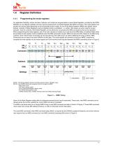
^ TIME BREAK □ DON'T CARE NOTE 1 This timing diagram shows C/A Parity Latency mode is “Disable” case. NOTE 2 List of MRS commands exception that do not apply to tMRD - Gear down mode - C/A Parity Latency mode - CS to Command/Address Latency mode - Per DRAM Addressability mode - VrefDQ training Value, VrefDQ Training mode and VrefDQ training Range Figure 3 — tMRD Timing Some of the Mode Register setting affect to address/command/control input functionality. These case, next MRS command can be allowed when the function updating by current MRS command completed. The MRS commands which do not apply...
Open the catalog to page 11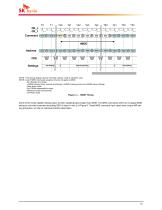
NOTE 1 This timing diagram shows CA Parity Latency mode is “Disable” case. NOTE 2 List of MRS commands exception that do not apply to tMOD - DLL Enable, DLL Reset - VrefDQ training Value, internal Vref Monitor, VrefDQ Training mode and VrefDQ training Range - Gear down mode - Per DRAM addressability mode - Maximum power saving mode - CA Parity mode Figure 4 — tMOD Timing Some of the mode register setting cases, function updating takes longer than tMOD. The MRS commands which do not apply tMOD timing to next valid command excluding DES is listed in note 2 of Figure 9. These MRS command input cases...
Open the catalog to page 12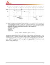
RTT_NOM tADC_min tADC_min tADC_max NOTE 1 NOTE 1 This timing diagram shows CA Parity Latency mode is “Disable” case. NOTE 2 NOTE 2 When an MRS command mentioned in this note affects RTT_NOM turn on timings, RTT_NOM turn off timings and RTT_NOM value, this means the MR register value changes. The ODT signal should set to be low for at least DODTLoff +1 clock before their affecting MRS command is issued and remain low until tMOD expires. The following MR registers affects RTT_NOM turn on timings, RTT_NOM turn off timings and RTT_NOM value and it requires ODT to be low when an MRS command change...
Open the catalog to page 13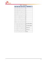
SK hynix Table 3 — CAS Latency
Open the catalog to page 15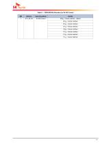
Table 6 — DDR4 MR Bit Allocation for Rx EQ Control
Open the catalog to page 17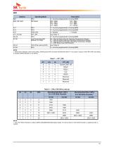
NOTE : 1. The 2 tCK Write Preamble is valid for DDR4-2400/2666/2933/3200 Speed Grade. For the 2nd Set of 2 tCK Write Preamble, no additional CWL is needed.
Open the catalog to page 18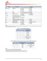
NOTE : 1. Write Command latency when CRC and DM are both enabled: 2. At less than or equal to 1600 then 4nCK; neither 5nCK nor 6nCK 3. At greater than 1600 and less than or equal to 2666 then 5nCK; neither 4nCK nor 6nCK 4. At greater than 2666 and less than or equal to 3200 then 6nCK; neither 4nCK nor 5nCK
Open the catalog to page 19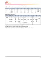
Table 11 — MPR Data Format NOTE : 1. MPR used for C/A parity error log readout is enabled by setting A[2] in MR3 2. For higher density of DRAM, where A[17] is not used, MPR2[1] should be treated as don’t care. 3. If a device is used in monolithic application, where C[2:0] are not used, then MPR3[2:0] should be treated as don’t care. 4. MPR3 bit 0~2 (CA parity latency) reflects the latest programmed CA parity latency values.
Open the catalog to page 20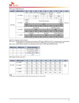
NOTE : 1. MPR page3 is specifically assigned to DRAM. Actual encoding method is vendor specific.
Open the catalog to page 21All SK hynix catalogs and technical brochures
 PC801
PC8012 Pages
 eMMC
eMMC2 Pages
 UFS
UFS1 Page
 CXL
CXL8 Pages
 MCP
MCP2 Pages
 DDR5 RDIMMs
2 Pages
 DDR5 DIMM for Server
2 Pages
 DDR SDRAM Device Operation
36 Pages
 DDR2 SDRAM Device Operations
62 Pages
 DDR3L SDRAM Device Operation
147 Pages
 NAND Flash
10 Pages
 Mobile Memory
5 Pages
 Graphics Memory
5 Pages
 Consumer Memory
7 Pages
 Computing Memory
24 Pages
 Product catalogue
12 Pages
 2013 Databook
28 Pages
