

DDR SDRAM Device Operation

DDR SDRAM Device Operation
Catalog excerpts

DDR SDRAM Device Operation List of Contents 1. Truth Table 3. Device Operation • Power-Up Sequence • Burst Read and Burst Write • Burst Read followed by Burst Read • Burst Write followed by Burst Write • Burst Read followed by Burst Write • Burst Write followed by Burst Read • Burst Read terminated by another Burst Read • Burst Write terminated by another Burst Write • Burst Read terminated by another Burst Write • Burst Write terminated by another Burst Read • Burst Read with Auto Precharge • Burst Write with Auto Precharge • Precharge command after Burst Read • Precharge command after Burst Write • Precharge termination of Burst Read • Precharge termination of Burst Write • DM masking (Write) • Burst Stop command (Read) • Auto Refresh and Precharge All command • Self Refresh Entry and Exit • Power Down mode • CKE function 6. Output Driver Characteristics 7. Timing Diagram • Data Input (Write) Timing • Data Output (Read) Timing • Power Down Mode • Auto Refresh Mode • Self Refresh Mode • Read without Auto Precharge • Read with Auto Pr
Open the catalog to page 1
DDR SDRAM Device Operation
Open the catalog to page 2
DDR SDRAM Device Operation
Open the catalog to page 3
DDR SDRAM Device Operation
Open the catalog to page 4
DDR SDRAM Device Operation 1. H - Logic High Level, L - Logic Low Level, X - Don't Care, V - Valid Data Input, BA - Bank Address, AP - AutoPrecharge Address, CA - Column Address, RA - Row Address, NOP - NO Operation. 2. All entries assume that CKE was active(high level) during the preceding clock cycle. 3. If both banks are idle and CKE is inactive(low level), then in power down mode. 4. Illegal to bank in specified state. Function may be legal in the bank indicated by Bank Address(BA) depending on the state of that bank. 5. If both banks are idle and CKE is inactive(low level), then self refresh...
Open the catalog to page 5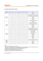
DDR SDRAM Device Operation Note: When CKE=L, all DQ and DQS must be in Hi-Z state. 1. CKE and /CS must be kept high for a minimum of 200 stable input clocks before issuing Read command. (See the parameter 'Exit Self Refresh to non-Read command' in AC CHARACTERISTICS for non-Read command) 2. All command can be stored after 2 clocks from low to high transition of CKE. 3. Illegal if CK is suspended or stopped during the power down mode. 4. Self refresh can be entered only from the all banks idle state. 5. Disabling CK may cause malfunction of any bank which is in active state.
Open the catalog to page 6
DDR SDRAM Device Operation SIMPLIFIED STATE DIAGRAM Pow er Applied Precharge PREALL Self Refresh REFS REFSX M RS Auto Refresh CKEL CKEH CKEH CKEL Burst Stop Precharge PREALL Autom atic Sequence Com m and Sequence PREALL = Precharge All Banks M RS = M ode Register Set EM RS = Extended M ode Register Set REFS = Enter Self Refresh REFSX = Exit Self Refresh REFA = Auto Refresh C KEL = Enter Pow er Dow n C KEH = Exit Pow er D ow n ACT = Active W rite A = W rite w ith Autoprecharge Read A = Read w ith Autoprecharge PRE = Precharge
Open the catalog to page 7
DDR SDRAM Device Operation POWER-UP SEQUENCE AND DEVICE INITIALIZATION DDR SDRAMs must be powered up and initialized in a predefined manner. Operational procedures other than those specified may result in undefined operation. Power must first be applied to Vdd, then to Vddq, and finally to Vref (and to the system VTT). VTT must be applied after VDDQ to avoid device latch-up, which may cause permanent damage to the device. VREF can be applied anytime after VDDQ, but is expected to be nominally coincident with VTT. Except for CKE, inputs are not recognized as valid until after Vref is applied....
Open the catalog to page 8
DDR SDRAM Device Operation 7. Issue 2 or more Auto Refresh commands. 8. Issue a Mode Register Set command to initialize the mode register with bit A8 = Low. Power-Up Sequence VDDQ tVTD Non-Read Command tXSRD* Power UP VDD and CK stable 2 or more Auto Refresh * 200 cycle(tXSRD) of CK are required (for DLL locking) before Read Command
Open the catalog to page 9
DDR SDRAM Device Operation Burst Read and Burst Write Burst Read and Burst Write commands are initiated as listed in Fig.1. Before the Burst Read command, the bank must be activated earlier. After /RAS to /CAS delay (tRCD), read operation starts. DDR SDRAM has been implemented with Data Strobe signal (DQS) which toggles high and low during burst with the same frequency as clock (CLK, /CLK). After CAS Latency (CL) which is defined as the interval between command clock and the first rising edge of the DQS, read data is launched onto data pin (DQ) with reference to DQS signal edge. Burst Write command...
Open the catalog to page 10
DDR SDRAM Device Operation Burst Read followed by Burst Read Back to back read operation in the same or different bank is possible as shown in Fig.2. Following first Read command, consecutive Read command can be initiated after BL/2 ticks of clock. In other words, minimum earliest possible Read command that does note interrupt the previous read data, can be issued after BL/2 clock is met. When Read(B) data out starts, data strobe signal does not transit to Hi-Z but toggle high and low for Read(B) data. Fig.2. Burst Read followed by Burst Read B urst length =4, C A S latency =2 Burst Write followed...
Open the catalog to page 11
DDR SDRAM Device Operation Burst Read followed by Burst Write Back to back read followed by write operation in the same or different bank is possible as shown in Fig.4. Following first Read command, consecutive Write command can be initiated after RU{CL+BL/2} ticks of clock. (RU=Round Up for half cycle of CAS latency, such as 1.5 and 2.5). In other words, minimum earliest possible Write command that does not interrupt the previous read data can be issued after RU{CL+BL/2} clock is met. Fig.4. Burst Read followed by Burst Write B urst length =4, C A S latency =2 Burst Write followed by Burst Read...
Open the catalog to page 12
DDR SDRAM Device Operation Burst Read terminated by another Burst Read Read command terminates the previous Read command and the data is available after CAS latency for the new command. Minimum delay from a Read command to next Read command is determined by /CAS to /CAS delay (tCCD). Timing diagram is shown in Fig.6. Fig.6. Burst Read terminated by another Burst Read R ead(A ) is term inated and R ead(B ) data out starts B urst length =4, C A S latency =2 Burst Write terminated by another Burst Write Write command terminates the previous Write command and the data is available after CAS latency...
Open the catalog to page 13All SK hynix catalogs and technical brochures
 PC801
PC8012 Pages
 eMMC
eMMC2 Pages
 UFS
UFS1 Page
 CXL
CXL8 Pages
 MCP
MCP2 Pages
 DDR5 RDIMMs
2 Pages
 DDR5 DIMM for Server
2 Pages
 DDR2 SDRAM Device Operations
62 Pages
 DDR3L SDRAM Device Operation
147 Pages
 DDR4 SDRAM Device Operation
266 Pages
 NAND Flash
10 Pages
 Mobile Memory
5 Pages
 Graphics Memory
5 Pages
 Consumer Memory
7 Pages
 Computing Memory
24 Pages
 Product catalogue
12 Pages
 2013 Databook
28 Pages
