- Catalogs
- Silicon Laboratories
- Si4730/Si4731/Si4734/Si4735-D60 Broadcast AM/FM/SW/LW Radio Receiver
Si4730/Si4731/Si4734/Si4735-D60 Broadcast AM/FM/SW/LW Radio Receiver
1 /42Pages

Si4730/Si4731/Si4734/Si4735-D60 Broadcast AM/FM/SW/LW Radio Receiver
1 /42Pages
Catalog excerpts

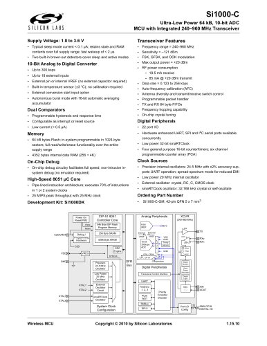
Si4730/31/34/35-D60 B ROADCAST AM/FM/SW/LW R ADIO R ECEIVER Features Ordering Information: See page 31. Pin Assignments Si473x-D60 (QFN) DFS Seven selectable AM channel filters AM/FM/SW/LW digital tuning EN55020 compliant No manual alignment necessary Programmable reference clock Adjustable soft mute control RDS/RBDS processor (Si4731/35) Digital audio out 2-wire and 3-wire control interface Integrated LDO regulator Wide range of ferrite loop sticks and air loop antennas supported QFN and SSOP packages RoHS compliant Worldwide FM band support (64–108 MHz) Worldwide AM band support (520–1710 kHz) SW band support (Si4734/35) (2.3–26.1 MHz) LW band support (Si4734/35) (153–279 kHz) Excellent real-world performance Integrated VCO Advanced AM/FM seek tuning Automatic frequency control (AFC) Automatic gain control (AGC) Digital FM stereo decoder Programmable de-emphasis Advanced Audio Processing Applications Table and portable radios Mini/micro systems CD/DVD and Blu-ray players Stereo boom boxes Modules for consumer electronics Clock radios Mini HiFi and docking stations Entertainment systems The Si473x-D60 digital CMOS AM/FM radio receiver IC integrates the complete broadcast tuner and receiver function from antenna input to digital audio output. The device leverages the Silicon Labs broadcast proven digital low-IF architecture, enabling a cost-effective, digital audio platform for consumer electronic applications with high TDMA noise immunity, superior radio performance, and high fidelity audio power amplification. Functional Block Diagram Copyright © 2013 by Silicon Laboratories This product, its features, and/or its architecture is covered by one or more of the following patents, as well as other patents, pending and issued, both foreign and domestic: 7,127,217; 7,272,373; 7,272,375; 7,321,324; 7,355,476; 7,426,376; 7,471,940; 7,339,503; 7,339,504.
Open the catalog to page 1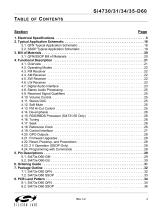
Si4730/31/34/35-D60 TABLE O F C ONTENTS Section 1. Electrical Specifications . . . . . . . . . . . . . . . . . . . . . . . . . . . . . . . . . . . . . . . . . . . . . . . . . . .5 2. Typical Application Schematic . . . . . . . . . . . . . . . . . . . . . . . . . . . . . . . . . . . . . . . . . . . . . 18 2.1. QFN Typical Application Schematic . . . . . . . . . . . . . . . . . . . . . . . . . . . . . . . . . . . . . 18 2.2. SSOP Typical Application Schematic . . . . . . . . . . . . . . . . . . . . . . . . . . . . . . . . . . . . 19 3. Bill of Materials . . . . . . . . . . . . . . . . . . . . ....
Open the catalog to page 3
Si4730/31/34/35-D60 9. Top Markings . . . . . . . . . . . . . . . . . . . . . . . . . . . . . . . . . . . . . . . . . . . . . . . . . . . . . . . . . . .37 9.1. Si473x-D60 Top Marking (QFN) . . . . . . . . . . . . . . . . . . . . . . . . . . . . . . . . . . . . . . . . 37 9.2. Top Marking Explanation (QFN) . . . . . . . . . . . . . . . . . . . . . . . . . . . . . . . . . . . . . . . . 37 9.3. Si473x-D60 Top Marking (SSOP) . . . . . . . . . . . . . . . . . . . . . . . . . . . . . . . . . . . . . . . 38 9.4. Top Marking Explanation (SSOP) . . . . . . . . . . . . . . . . . . . . . . . . . . . ....
Open the catalog to page 4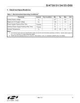
Si4730/31/34/35-D60 1. Electrical Specifications Table 1. Recommended Operating Conditions1 Parameter Test Condition Analog Supply Voltage Digital and I/O Supply Voltage Power Supply Powerup Rise Time Interface Power Supply Powerup Rise Time Ambient Temperature Notes: 1. All minimum and maximum specifications apply across the recommended operating conditions. Typical values apply at VA = 3.3 V and 25 C unless otherwise stated. 2. SSOP devices operate down to 2 V at 25 °C. See section “4.23. 2 V Operation (SSOP Only)” for details.
Open the catalog to page 5
Test Condition FM Mode VAQFN Supply Current VDQFN Supply Current VASSOP Supply Current VDSSOP Supply Current VAQFN Supply Current VDQFN Supply Current VASSOP Supply Current VDSSOP Supply Current AM Mode VAQFN Supply Current VDQFN Supply Current VASSOP Supply Current VDSSOP Supply Current VAQFN Supply Current VDQFN Supply Current VASSOP Supply Current VDSSOP Supply Current SCLK, RCLK inactive SCLK, RCLK inactive Digital Output Mode Analog Output Mode Powerdown VAQFN Powerdown Current VASSOP Powerdown Current VDQFN Powerdown Current VDSSOP Powerdown Current IAPD IDPD High Level Input Voltage3 High...
Open the catalog to page 6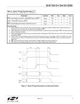
Si4730/31/34/35-D60 Table 3. Reset Timing Characteristics1,2,3 (VA = 2.7 to 5.5 V, VD = 1.62 to 3.6 V, TA = –20 to 85 °C) RST Pulse Release time before VDD/VIO turn off RST Pulse Width and GPO1, GPO2/INT Setup to Important Notes: 1. When selecting 2-wire mode, the user must ensure that a 2-wire start condition (falling edge of SDIO while SCLK is high) does not occur within 300 ns before the rising edge of RST. 2. When selecting 2-wire mode, the user must ensure that SCLK is high during the rising edge of RST, and stays high until after the first start condition. 3. When selecting 3-wire mode,...
Open the catalog to page 7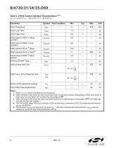
Si4730/31/34/35-D60 Table 4. 2-Wire Control Interface Characteristics1,2,3 (VA = 2.7 to 5.5 V, VD = 1.62 to 3.6 V, TA = –20 to 85 °C) Test Condition SCLK Frequency SCLK High Time SCLK Input to SDIO Setup (START) SCLK Input to SDIO Hold (START) SDIO Input to SCLK Setup SDIO Input to SCLK Hold4,5 SCLK input to SDIO Setup (STOP) STOP to START Time SDIO Output Fall Time SDIO Input, SCLK Rise/Fall Time tf:IN tr:IN SCLK, SDIO Capacitive Loading Input Filter Pulse Suppression Notes: 1. When VD = 0 V, SCLK and SDIO are low impedance. 2. When selecting 2-wire mode, the user must ensure that a 2-wire start...
Open the catalog to page 8
tf:IN, tf:OUT tHD:DAT tSU:DAT Figure 2. 2-Wire Control Interface Read and Write Timing Parameters SDIO START Figure 3. 2-Wire Control Interface Read and Write Timing Diagram
Open the catalog to page 9
Si4730/31/34/35-D60 Table 5. 3-Wire Control Interface Characteristics (VA = 2.7 to 5.5 V, VD = 1.62 to 3.6 V, TA = –20 to 85 °C) Test Condition SCLK Frequency SCLK High Time SDIO Input to SCLKHold SCLKto SDIO Output Valid SCLKto SDIO Output High Z SCLK, SEN, SDIO, Rise/Fall time SDIO Input, SEN to SCLKSetup Note: When selecting 3-wire mode, the user must ensure that a rising edge of SCLK does not occur within 300 ns before the rising edge of RST. Figure 4. 3-Wire Control Interface Write Timing Parameters Figure 5. 3-Wire Control Interface Read Timing Parameters
Open the catalog to page 10All Silicon Laboratories catalogs and technical brochures
 ISOmodem Solutions Guide
2 Pages
 PRODUCT SELECTOR GUIDE 2013
36 Pages
 MCU Selector Guide
20 Pages
 Wireless and RF Selector Guide
12 Pages
 Human Interface Solutions Guide
12 Pages
 Isolation Selector Guide
10 Pages
 Microcontroller Selector Guide
20 Pages
 Audio Applications Guide
24 Pages
 USB Bridge Solutions
2 Pages
 Si4032/31/30 ISM Transmitter
2 Pages


Archived catalogs
 Broadcast Audio Solutions
2 Pages
 Digital Power Solutions
2 Pages
 Low-Voltage/Low-Power MCUs
2 Pages


- Liebherr temperature sensor
- Proximity switch
- Transceiver module
- Rectangular proximity sensor
- Crystal oscillator
- Radio transceiver module
- Surface-mount oscillator
- IC transceiver
- Semiconductor temperature sensor
- Electromechanical oscillator
- Digital proximity sensor
- Gate driver
- Silicon temperature sensor
- Signal isolator-converter
- FM transceiver
- Infrared proximity sensor
- MOSFET gate driver
- Isolator signal isolator-converter
- IC temperature sensor
- Opto-isolated gate driver