- Catalogs
- Silicon Laboratories
- Si4136/Si4126 ISM RF SYNTHESIZER WITH INTEGRATED VCOS FOR WIRELESS COMMUNICATIONS
Si4136/Si4126 ISM RF SYNTHESIZER WITH INTEGRATED VCOS FOR WIRELESS COMMUNICATIONS
Si4136/Si4126 ISM RF SYNTHESIZER WITH INTEGRATED VCOS FOR WIRELESS COMMUNICATIONS
- Dual-band RF synthesizers: RF1 (2300-2500 MHz), RF2 (2025-2300 MHz)
- IF synthesizer range: 62.5 MHz to 1000 MHz
- Integrated VCOs, loop filters, varactors, and resonators
- Low phase noise and minimal external components required
- Operates at 2.7 V to 3.6 V
- Available in 24-pin TSSOP and 28-lead QFN packages
- Operating temperature: -40°C to 85°C
- Supply voltage: 2.7 V to 3.6 V
- DC supply voltage: -0.5 to 4.0 V
- Input current: ±10 mA
- Storage temperature range: -55°C to 150°C
- Register 4: RF2 N Divider, with a minimum value of 240.
- Register 5: IF N Divider, with a minimum value of 56.
- Register 6: RF1 R Divider, with values ranging from 7 to 8189 depending on KP1 settings.
- Register 7: RF2 R Divider, with values ranging from 7 to 8189 depending on KP2 settings.
- Register 8: IF R Divider, with values ranging from 7 to 8189 depending on KP1 settings.
- Si4136-BT/GT: Includes pins for serial clock input, serial data input, RF output, auxiliary output, and various supply voltages.
- Si4136-BM/GM: Similar to the BT/GT variant but with additional pins for serial port enable and data input.
Catalog excerpts

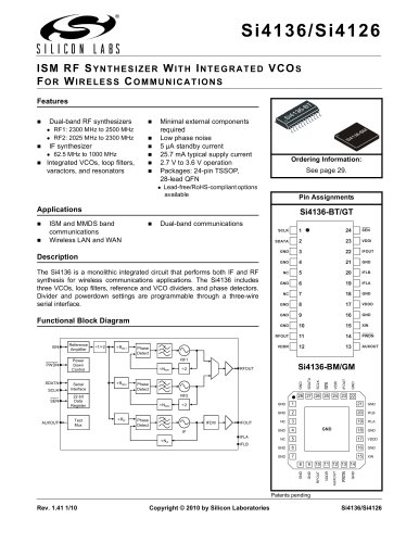
Rev. 1.41 1/10 Copyright © 2010 by Silicon Laboratories Si4136/Si4126 Si4136/Si4126 ISM RF SYNTHESIZER WITH INTEGRATED VCOS FOR WIRELESS COMMUNICATIONS Features Applications Description The Si4136 is a monolithic integrated circuit that performs both IF and RF synthesis for wireless communications applications. The Si4136 includes three VCOs, loop filters, reference and VCO dividers, and phase detectors. Divider and powerdown settings are programmable through a three-wire serial interface. Functional Block Diagram ƒÞ Dual-band RF synthesizers ƒÜƒnRF1: 2300 MHz to 2500 MHz ƒÜƒnRF2: 2025 MHz to 2300 MHz ƒÞ IF synthesizer ƒÜƒn62.5 MHz to 1000 MHz ƒÞ Integrated VCOs, loop filters, varactors, and resonators ƒÞ Minimal external components required ƒÞ Low phase noise ƒÞ 5 ìA standby current ƒÞ 25.7 mA typical supply current ƒÞ 2.7 V to 3.6 V operation ƒÞ Packages: 24-pin TSSOP, 28-lead QFN ƒÜƒnLead-free/RoHS-compliant options available ƒÞ ISM and MMDS band communications ƒÞ Wireless LAN and WAN ƒÞ Dual-band communications IFOUT IFLA IFLB RFOUT XIN PWDN SDATA SCLK SEN IF RF2 RF1 AUXOUT Phase Detect Phase Detect „i2 „i2 Phase IFDIV Detect Test Mux 22-bit Data Register Serial Interface Power Down Control Reference Amplifier „iRRF1 „iRRF2 „iRIF „iNRF1 „iNRF2 „iNIF ÷1/÷2 Patents pending Ordering Information: See page 29. Pin Assignments Si4136-BT/GT Si4136-BM/GM SCLK SDATA GND GND NC GND NC GND GND GND RFOUT VDDR SEN VDDI IFOUT GND IFLB IFLA GND VDDD GND XIN PWDN AUXOUT 1 2 3 4 5 6 7 8 9 10 11 12 24 23 22 21 20 19 18 17 16 15 14 13 SCLK SDATA GND GND NC NC GND GND RFOUT VDDR SEN VDDI IFOUT GND IFLB IFLA GND VDDD GND XIN PWDN AUXOUT 21 20 19 18 17 16 15 8 9 10 11 12 13 14 28 27 26 25 24 23 22 1 2 3 4 5 6 7 GND GND GND GND GND GND GND
Open the catalog to page 1
Si4136/Si4126 Rev. 1.41 3 TABLE OF CONTENTS Section Page 1. Electrical Specifications . . . . . . . . . . . . . . . . . . . . . . . . . . . . . . . . . . . . . . . . . . . . . . . . . . .4 2. Functional Description . . . . . . . . . . . . . . . . . . . . . . . . . . . . . . . . . . . . . . . . . . . . . . . . . . .16 2.1. Serial Interface . . . . . . . . . . . . . . . . . . . . . . . . . . . . . . . . . . . . . . . . . . . . . . . . . . . . .16 2.2. Setting the IF VCO Center Frequencies . . . . . . . . . . . . . . . . . . . . . . . . . . . . . . . . . .16 2.3. Self-Tuning Algorithm . . . . ....
Open the catalog to page 3
Si4136/Si4126 4 Rev. 1.41 1. Electrical Specifications Table 1. Recommended Operating Conditions Parameter Symbol Test Condition Min Typ Max Unit Ambient Temperature TA –40 25 85 °C Supply Voltage VDD 2.7 3.0 3.6 V Supply Voltages Difference Vƒ´ (VDDR – VDDD), (VDDI – VDDD) –0.3 — 0.3 V Note: All minimum and maximum specifications are guaranteed and apply across the recommended operating conditions. Typical values apply at nominal supply voltages and an operating temperature of 25°C unless otherwise stated. Table 2. Absolute Maximum Ratings1,2 Parameter Symbol Value Unit DC Supply Voltage VDD...
Open the catalog to page 4
Si4136/Si4126 Rev. 1.41 5 Table 3. DC Characteristics (VDD = 2.7 to 3.6 V, TA = –40 to 85 °C) Parameter Symbol Test Condition Min Typ Max Unit Total Supply Current1 RF1 and IF operating — 25.7 31 mA RF1 Mode Supply Current1 — 15.7 19 mA RF2 Mode Supply Current1 — 15 18 mA IF Mode Supply Current1 — 10 12 mA Standby Current PWDN = 0 — 1 — ìA High Level Input Voltage2 VIH 0.7 VDD — — V Low Level Input Voltage2 VIL — — 0.3 VDD V High Level Input Current2 IIH VIH = 3.6 V, VDD = 3.6 V –10 — 10 ìA Low Level Input Current2 IIL VIL = 0 V, VDD= 3.6 V –10 — 10 ìA High Level Output Voltage3 VOH IOH = –500...
Open the catalog to page 5
Si4136/Si4126 6 Rev. 1.41 Figure 1. SCLK Timing Diagram Table 4. Serial Interface Timing (VDD = 2.7 to 3.6 V, TA = –40 to 85 °C) Parameter1 Symbol Test Condition Min Typ Max Unit SCLK Cycle Time tclk Figure 1 40 — — ns SCLK Rise Time tr Figure 1 — — 50 ns SCLK Fall Time tf Figure 1 — — 50 ns SCLK High Time th Figure 1 10 — — ns SCLK Low Time tl Figure 1 10 — — ns SDATA Setup Time to SCLK„^2 tsu Figure 2 5 — — ns SDATA Hold Time from SCLK„^2 thold Figure 2 0 — — ns SEN„` to SCLK„^ƒnDelay Time2 ten1 Figure 2 10 — — ns SCLK„^ to SEN„^ƒnDelay Time2 ten2 Figure 2 12 — — ns SEN„^ to SCLK„^ƒnDelay Time2...
Open the catalog to page 6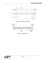
Si4136/Si4126 Rev. 1.41 7 Figure 2. Serial Interface Timing Diagram Figure 3. Serial Word Format A A D 17 D 16 D 15 D 14 D 13 D 12 D 11 D 10 D9 D8 D7 D6 D5 D4 D3 D2 D1 D0 A3 A2 A1 First bit clocked in Last bit clocked in address field A0 data field
Open the catalog to page 7
Si4136/Si4126 8 Rev. 1.41 Table 5. RF and IF Synthesizer Characteristics (VDD = 2.7 to 3.6 V, TA = –40 to 85 °C) Parameter1 Symbol Test Condition Min Typ Max Unit XIN Input Frequency fREF XINDIV2 = 0 2 — 25 MHz XIN Input Frequency fREF XINDIV2 = 1 25 — 50 MHz Reference Amplifier Sensitivity VREF 0.5 — VDD +0.3 V VPP Phase Detector Update Frequency fƒÖ fƒÖƒn= fREF/R for XINDIV2 = 0 fƒÖƒn= fREF/2R for XINDIV2 = 1 0.010 — 1.0 MHz RF1 VCO Tuning Range2 2300 — 2500 MHz RF2 VCO Tuning Range2 2025 — 2300 MHz IF VCO Center Frequency Range fCEN 526 — 952 MHz IFOUT Tuning Range from fCEN with IFDIV 62.5...
Open the catalog to page 8
Si4136/Si4126 Rev. 1.41 9 RF1 Harmonic Suppression Second Harmonic — –28 –20 dBc RF2 Harmonic Suppression — –23 –20 dBc IF Harmonic Suppression — –26 –20 dBc RFOUT Power Level ZL = 50ƒnƒÇƒzƒnRF1 active –7 –3.5 –0.5 dBm RFOUT Power Level ZL = 50ƒnƒÇƒzƒnRF2 active –7 –3.5 –0.5 dBm IFOUT Power Level ZL = 50 ƒÇ –7 –4 0 dBm RF1 Output Reference Spurs Offset = 1 MHz — –63 — dBc Offset = 2 MHz — –68 — dBc Offset = 3 MHz — –70 — dBc RF2 Output Reference Spurs Offset = 1 MHz — –63 — dBc Offset = 2 MHz — –68 — dBc Offset = 3 MHz — –70 — dBc Powerup Request to Synthesizer Ready3 Time tpup Figures 4, 5 fƒÖƒn>...
Open the catalog to page 9All Silicon Laboratories catalogs and technical brochures
 ISOmodem Solutions Guide
2 Pages
 PRODUCT SELECTOR GUIDE 2013
36 Pages
 MCU Selector Guide
20 Pages
 Wireless and RF Selector Guide
12 Pages
 Human Interface Solutions Guide
12 Pages
 Isolation Selector Guide
10 Pages
 Microcontroller Selector Guide
20 Pages
 Audio Applications Guide
24 Pages
 USB Bridge Solutions
2 Pages
 Si4032/31/30 ISM Transmitter
2 Pages


Archived catalogs
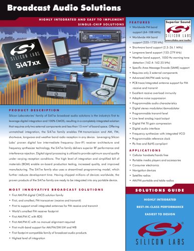 Broadcast Audio Solutions
2 Pages
 Digital Power Solutions
2 Pages
 Low-Voltage/Low-Power MCUs
2 Pages


- Temperature probe
- Proximity switch
- Transceiver module
- Rectangular proximity sensor
- Crystal oscillator
- Radio transceiver module
- Surface-mount oscillator
- IC transceiver
- Semiconductor temperature sensor
- Electromechanical oscillator
- Digital proximity sensor
- Gate driver
- Silicon temperature sensor
- Signal isolator-converter
- FM transceiver
- Infrared proximity sensor
- MOSFET gate driver
- Isolator signal isolator-converter
- IC temperature sensor
- Opto-isolated gate driver