Catalog excerpts

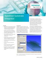
Xpedition Substrate Integrator Benefits • Rapid planning, prototyping and optimization of 2.5/3D heterogeneously integrated die/chiplets based semiconductor package assemblies • System connectivity management and visualization with cross-domain pin/signal mapping/shorting and system-level logical verification Introduction Xpedition® Substrate Integrator (xSI) provides a graphical, rapid virtual prototyping environment tuned for the exploration and integration of multiple heterogeneous ICs/chiplets and interposers into High Density Advanced Packages (HDAP). It utilizes a System Technology Co-Optimization (STCO) methodology to co-design complex 2.5/3D package assemblies while targeting different system PCBs. Designers and micro-architects can quickly and easily assemble complete cross-domain substrate systems and drive ball map plans and pin optimization through a rule-based methodology. Using an STCO methodology ensures ICs, packages, and PCBs are optimized in the context of each other. This results in fewer layers and tighter control of the design process resulting in optimized device performance, lower-cost package assemblies and PCBs with the benefit of system level performance. • User-definable rules for custom optimization of pin and ball-out assignments • Single-window visualization and hierarchical management of multi- die/ chiplet and substrate assemblies • Pin-based interface planning with or without nets. • Extensive input and output data formats • System-level LVS/STA verification through Calibre® 3DSTACK • Integration with Xpedition Package Designer and Calibre, for detailed implementation, verification, and signoff Figure 1: Complex heterogeneous 2.5/3D assemblies can be defined, managed and optimized for one or multiple target system PCBs
Open the catalog to page 1
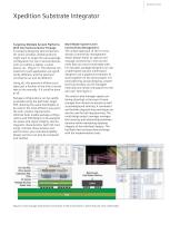
Xpedition Substrate Integrator Targeting Multiple System Platforms With One Semiconductor Package A company designing semiconductors for smart, wireless, mobile products might want to target the same package configuration for use in several devices, such as a tablet, a laptop, a smart phone, etc. (Figure 1). The physical constraints for each application are significantly different, and the electrical constraints can also be different. Using xSI, this process is efficient and takes just a fraction of the time it would take to do manually, if it could be done at all. Package configurations...
Open the catalog to page 2
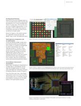
Prototyping & Planning Determining the best package based on cost and performance often requires the development of a custom package definition. In some cases, this can be a simple case of ball/pin depopulation. As an example, a CPU or GPU may require a completely asymmetrical array of pins to satisfy its market needs. Shown in Figure 3, xSI contains powerful capabilities to dynamically add, delete, copy, move, and adjust pin pitch. Heterogeneous Integration and Co-optimization Virtual Die Models (VDM) enable early asynchronous planning and optimization of ASICs or chiplets by...
Open the catalog to page 3
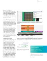
Rules Driven Pin Planning An easy-to-use pin planning and optimization rules engine lets engineers define which pins on the package can have which signals or interfaces assigned to them. Rules can also be written to ensure that critical nets are assigned adjacent to ground nets or that corner pins will only accept the ground signal. Figure 6 shows how rules are reflected in colors that designate which rule applies to a particular ball. Several types of rules are illustrated. For example, if data busses were not allowed on inner pins, any attempt to do so would result in an error reflected...
Open the catalog to page 4All SIEMENS EDA catalogs and technical brochures
-
Calibre nmDRC
4 Pages
Archived catalogs
-
Tessent Connect
3 Pages
-
Calibre LFD
3 Pages
-
Vista Virtual Prototyping
4 Pages
-
Vista Architect
4 Pages
-
Tessent IJTAG
2 Pages
-
Calibre® MPCpro
2 Pages
-
LeonardoSpectrum
4 Pages
-
Oasys-RTL
3 Pages
-
Olympus-SoC
5 Pages
-
ICanalyst
4 Pages
-
Calibre RVE
3 Pages
-
Calibre nmLVS
3 Pages
-
Calibre LFD
3 Pages
-
Tanner L-Edit IC Layout
4 Pages
-
Tanner Designer
2 Pages
-
Tanner Waveform Viewer
2 Pages
-
Tanner T-Spice Simulation
2 Pages
-
ReqTracer
2 Pages
-
LeonardoSpectrum™
4 Pages
-
HDL Designer
2 Pages
-
Nucleus RTOS
2 Pages
-
Calibre ® MPCpro
2 Pages
-
Calibre OPC and PSM
6 Pages
-
Multicore Framework
2 Pages
-
Volcano VSTAR Ethernet
2 Pages
-
Volcano VSTAR AUTOSAR
2 Pages
-
CAT/TransCable
2 Pages
-
ReadyStart?
2 Pages
-
Inflexion UI
2 Pages
-
TransDesign
6 Pages
-
TransCable
2 Pages
-
TranSACT
2 Pages
-
TransOVM
2 Pages
-
TransBridge
2 Pages
-
Calibre xACT 3D
2 Pages
-
Volcano? VSA
2 Pages
-
Calibre xRC
3 Pages
-
Calibre xRC-CB
2 Pages
-
ces-ds
2 Pages
-
VolcanoBootloader
2 Pages
-
flovent
12 Pages
-
flotherm
8 Pages
-
floefd
12 Pages
-
Calibre DESIGNrev
2 Pages
-
Calibre xL
2 Pages
-
Calibre nmDRC
4 Pages
-
ADiT
2 Pages
-
Calibre RealTime
2 Pages
-
Questa ADMS
7 Pages
-
iSolve DigIQ Interface
2 Pages
-
Questa® Codelink Turbo
3 Pages
-
RC250
2 Pages
-
RC340
2 Pages
-
Atmel SAM9263
2 Pages
-
Sourcery Analyzer
2 Pages
-
Capital Migration Services
2 Pages
-
Capital Harness MPM
2 Pages
-
Vista
4 Pages
-
Capital ModularXC
2 Pages
-
Capital HarnessXC
2 Pages
-
Capital Integrator
2 Pages
-
Capital Logic
2 Pages
-
Volcano Bootloader
2 Pages
-
Calibre® OPCverify™
2 Pages
-
Nucleus
2 Pages
-
Mentor Embedded Linux
10 Pages
-
PADS AutoRouter
4 Pages
-
Board Station XE (BSXE
9 Pages
-
Board Architect
2 Pages
-
PADS Suites
3 Pages
-
AccuSim II
2 Pages
-
AccuParts™
1 Pages
-
FloVENT
12 Pages
-
FloTHERM PCB
2 Pages
-
FloTHERM® IC
2 Pages
-
Calibre OPCverify
2 Pages
-
Olympus-SoC
2 Pages
-
Catapult C Synthesis
4 Pages
-
NUCLEUS RTOS SOLUTIONS
2 Pages
-
EDGE Developer Suite
2 Pages
-
MAJIC JTAG Probe
3 Pages
-
Mentor Embedded Inflexion UI
2 Pages
-
CHS
4 Pages
-
VeSys
2 Pages
-
TransLayout™
2 Pages
-
PCB Systems Board Station XE
4 Pages
-
Mechanical Analysis FloEFD
7 Pages
-
Calibre nmOPC
2 Pages


