- Company
- Products
- Catalogs
- News & Trends
- Exhibitions
HG185FH005
1 /21Pages

HG185FH005
1 /21Pages
Catalog excerpts
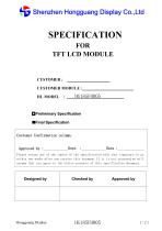
Shenzhen Hongguang Display Co.,Ltd CUSTOMER : CUSTOMER MODULE : HL MODEL Preliminary Specification ■Final Specification Customer Confirmation column: Approved by : Please return one of the copies of the specification with your signature to us within two weeks after you receive this document.If it is not returned,we will assume that you agree to the entire contents of this specification document. Hongguang Display
Open the catalog to page 1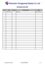
Shenzhen Hongguang Display Co.,Ltd REVISION HISTORY Rev Hongguang Display Revision Items Final spec Editor Tianyao. Zhang
Open the catalog to page 2
Shenzhen Hongguang Display Co.,Ltd CONTENTS 1. Hongguang Display
Open the catalog to page 3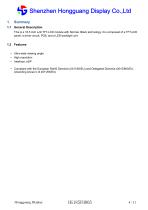
Shenzhen Hongguang Display Co.,Ltd 1. 1.1 General Description This is a 18.5 inch a-Si TFT-LCD module with Normal- Black technology. It is composed of a TFT-LCD panel, a driver circuit, PCB, and a LED backlight unit. 1.2 Features • Ultra-wide viewing angle • High resolution • Interface: eDP • Compliant with the European RoHS Directive (2011/65/EU) and Delegated Directive (2015/863/EU, Amending Annex II of 2011/65/EU) Hongguang Display
Open the catalog to page 4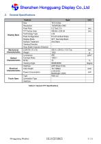
Shenzhen Hongguang Display Co.,Ltd 2. General Specifications Feature Display Spec Mechanical Characteristics Optical Characteristics Electrical Characteristics Touch Spec Size Resolution Pixel Pitch TFT Active Area Technology Type Pixel Configuration Display Mode Surface Treatment Viewing Direction Gray Scale Inversion Direction 18.5 inches 1920(RGB)x1080 0.213x0.213 408.96 x 230.04 a-Si R.G.B Vertical Stripe SFT, Normally Black Anti-Glare - LCM (W x H x D) Weight Luminance Contrast Ratio NTSC Viewing Angle Interface Color Depth Power Consumption Type Lamination Type Interface Table 2.1 General...
Open the catalog to page 5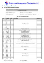
Shenzhen Hongguang Display Co.,Ltd 3. Input / Output Terminals 3.1 CN1 Pin assignment (LCD Interface) Connector Information LCD Module connector Matching connector 20454-240T (IPEX, HOUSING) or equivalent Table 3.1.1 Connector information High Speed Ground Complement Signal Link Lane 1 True Signal Link Lane 1 High Speed Ground Complement Signal Link Lane 0 True Signal Link Lane 0 Hongguang Display Keep this pin open High Speed Ground True Signal Auxiliary Channel Complement Signal Auxiliary Channel High Speed Ground Power supply for LCD panel signal processing board Keep this pin Open. Ground...
Open the catalog to page 6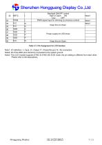
Shenzhen Hongguang Display Co.,Ltd 32 Backlight ON/OFF control High or Open: ON Low: OFF PWM signal input for dimming (Luminance control) Keep this pin Open. Power supply for LED driver Keep this pin Open. Table 3.1.2 Pin Assignment for LCD Interface Note1: I/O definition: I---Input, O---Output, P---Power/Ground, N---No connection Note2: All of the GND pins should be connected to the system ground. Note3: This LCD module supports SYNC & SYNC-DE & DE mode, the pin setting is different from each other. Please refer to the descriptions. Hongguang Display
Open the catalog to page 7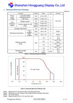
Shenzhen Hongguang Display Co.,Ltd 4. Absolute Maximum Ratings GND=0V Parameter Display signals Function signal for LED driver LCD panel signal processing board LED driver Power supply voltage Input voltage for signals Storage temperature Front surface Rear surface Operating temperature Table 4.1 Absolute Maximum Ratings Table 4.2 Absolute Maximum Ratings chart Measured at LCD panel surface (including self-heat) Measured at LCD module's rear shield surface (including self-heat) No condensation Water amount at Ta= 70°C and RH=
Open the catalog to page 8
Shenzhen Hongguang Display Co.,Ltd 5. Electrical Characteristics 5.1 DC Characteristics for Panel Driving Item Power supply voltage Power supply current Permissible ripple voltage Power Consumption at VCC= 5.0V for VCC Black pattern Table 5.1.1 Operating Voltages Note1: Indicated the subsequent version may be updated. 5.2 DC Characteristics for Backlight Driving Item Forward Current Voltage Forward Current Permissible ripple voltage Backlight Power WBL Consumption High Input voltage for PWM signal Low High Input voltage for BRTC signal Low High Input current for PWM signal Low High Input current...
Open the catalog to page 9
Shenzhen Hongguang Display Co.,Ltd 5.3 Recommended Power ON/OFF Sequence 5.3.1 LCD panel signal processing board T2 50ms VCC Note 1 0V AUX 0V Main link Note 2 0V LCD Link Trinning T5 50ms Video from source black 200ms T6 Note1: T1< T2. Note2: The low level of these signals and analog powers are GND level. Note3: All of the power and signals should be kept at GND level before power on. If there are residual voltages on them, the LCD might not work properly. Note4: The power on/off sequence is the first version. It will be updated when the design is fixed. Note5: BL is the voltage applied...
Open the catalog to page 10
Shenzhen Hongguang Display Co.,Ltd 5.4 LCD Module Block Diagram 5.4.1 Block Diagram Host AUX_CH_P AUX_CH_N Power supply for gradation DC/DC converter Controller with receiver for eDP EEPROM for EDID and Timing-Controller LCD panel signal processing board Figure 5.5.1 LCD Module Block Diagram Note1: Relation between H_GND (High Speed Ground), GND (Signal ground), GNDB (LED driver ground) and FG (Frame ground) in the LCD module are as follows. H_GND- GND H_GND- GNDB H_GND- FG GND- GNDB GND- FG GNDB- FG Connected Connected Connected Connected Connected Connected Note2: H_GND, GND, GNDB and FG must...
Open the catalog to page 11
Shenzhen Hongguang Display Co.,Ltd 5.4.2 eDP SIGNAL TIMING SPECIFICATIONS 5.4. Display port main link signal Jitter tracking bandwidth Link clock down spreading Unit interval Cycle-toCycle jitter time Differential peak-to-peak input voltage Rx input DC common mode voltage 5.4.2 Display port HPD signal Description Hot plug detect 5.4.3 Display port AUX signal Description AUX differential peak-to-peak voltage When driving AUX differential peak-to-peak voltage When receiving AUX common-mode voltage When transmitting AUX common-mode voltage When receiving AUX differential termination resistance Hongguang...
Open the catalog to page 12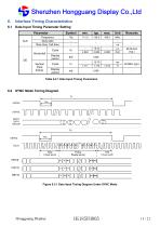
Shenzhen Hongguang Display Co.,Ltd 6. Interface Timing Characteristics 6.1 Data Input Timing Parameter Setting Parameter CLK Frequency Duty ratio Rise time, Fall time Horizontal Display period Display period Table 6.2.1 Data Input Timing Parameters 6.2 SYNC Mode Timing Diagram Figure 6.3.1 Data Input Timing Diagram Under SYNC Mode Hongguang Display
Open the catalog to page 13All Shenzhen Hongguang Display Co., Ltd catalogs and technical brochures
 HG215FH008T01
30 Pages
 HG170SX006T01
20 Pages
 HG160WQ004
64 Pages
 HG156FH011
23 Pages
 HG133FH017T01
32 Pages
 HG121WX001T01
22 Pages
 HG116FH008
24 Pages
 HG104SV003
27 Pages
 HG101WX054
12 Pages
 HG101WX053
12 Pages
 HG101WX049
38 Pages
 HG101WX047T01
19 Pages
 HG101WX047
19 Pages
 HG101WX046
18 Pages
 HG101WX030
24 Pages
 HG101WX028
21 Pages
 HG101WX026T01
20 Pages
 HG101WX025
19 Pages
 HG101WX022
19 Pages
 HG101WX021T01
20 Pages
 HG101WX021
20 Pages
 HG050WV038
18 Pages
 HG101WX019T01
20 Pages
 HG101WX019
20 Pages
 HG101WX016
20 Pages
 HG101WX005T01
22 Pages
 HG101WU076
25 Pages
 HG101WU072T01
23 Pages
 HG101WU072
23 Pages
 HG101WU065
23 Pages
 HG101WU063
24 Pages
 HG101WU062
27 Pages
 HG101WU039
30 Pages
 HG101WU035
23 Pages
 HG101WU032T01
18 Pages
 HG101WU013
17 Pages
 HG101WU010
17 Pages
 HG101WU008T01
17 Pages
 HG101WS045
22 Pages
 HG101WS042
17 Pages
 HG101WS040
19 Pages
 HG101WQ004T01
13 Pages
 HG101WQ003
13 Pages
 HG097XG006T01
17 Pages
 HG097QX005
17 Pages
 HG097QX003Z05
18 Pages
 HG097QX003T02
18 Pages
 HG097QX003T01
18 Pages
 HG090WS008
19 Pages
 HG080WX034
19 Pages
 HG080WX032
12 Pages
 HG080WX015
19 Pages
 HG080WX013
19 Pages
 HG080WV029
20 Pages
 HG080WV027
22 Pages
 HG080WU018T01
19 Pages
 HG080WU009
14 Pages
 HG070WX006
13 Pages
 HG070WX005
19 Pages
 HG070WS051T01
19 Pages
 HG070WV048
23 Pages
 HG070WV047
23 Pages
 HG070WV037R01
20 Pages
 HG070WV035T01
19 Pages
 HG070WV035
18 Pages
 HG070WV031
12 Pages
 HG070WV026
23 Pages
 HG070WV022
23 Pages
 HG070WV020
12 Pages
 HG070WV013T01
20 Pages
 HG070WV013R02
20 Pages
 HG070WU039
25 Pages
 HG070WS055
14 Pages
 HG070WS052
13 Pages
 HG070WV051T01
19 Pages
 HG070WS050
22 Pages
 HG070WS049T02
13 Pages
 HG070WS049T01
13 Pages
 HG070WS049-V1
21 Pages
 HG070WS048
25 Pages
 HG070WS046T03
13 Pages
 HG050HD030-V3
18 Pages
 HG215FH008T02
30 Pages
 HG104SV004
21 Pages
 HG050HD030T01
18 Pages
Archived catalogs
 HG043HV026
16 Pages
 HG024QV023R01
1 Page
 HG030FH006T02
16 Pages
 HG055FH018T01
20 Pages
 HG055HD017
16 Pages
 HG055FH021
20 Pages
 HG005WS003
39 Pages
 HG007WS003
50 Pages
 HG010WZ003
50 Pages
 HG015WZ003
49 Pages
 HG080STD02C
7 Pages
 HG104VG002-V0
20 Pages
 HG215FH008
30 Pages
 HG097XG008
17 Pages
 HGYD2690H-V1
21 Pages
 HG173FH002G01
30 Pages
 HG173FH002
30 Pages
 HG043HV002T02
17 Pages
 HG050WV009
19 Pages
 HG028HS003
15 Pages
 HG032WV001
17 Pages
 HG032XG003
19 Pages
 HG034SV004
14 Pages
 HG035SV003
22 Pages
 HG039WV004
19 Pages
 HG040HH005
16 Pages
 HG040HS002T01
16 Pages
 HG040WV006T02
18 Pages
 HG043HV002P01
10 Pages
 HG043HV002R03
17 Pages
 HG043WV005T01
19 Pages
 HG140FH005
20 Pages
 HG043HV008
17 Pages
 HG043HV008T01
17 Pages
 HG043HV009
21 Pages
 HG043HV010
21 Pages
 HG050WV010
19 Pages
 HG030FW006
14 Pages
 HG043HV022
16 Pages
 HG043HV028
20 Pages
 HG043WV016
18 Pages
 HG043WV023T01
19 Pages
 HG043HV029
19 Pages
 HG080WX039-V0
19 Pages
 HG050FH028T02
18 Pages
 HG050HD026T01
18 Pages
 HG101WU042-V0
29 Pages
 HG060HD012
18 Pages
 HG025HV006
12 Pages
 HG050QZ002
21 Pages
 HG050WV005
18 Pages
 HG050WV005T01
18 Pages
 HG050WV008T01
20 Pages
 HG050WV09G01
19 Pages
 HG050WV032
10 Pages
 HG050WV032T01
10 Pages
 HG050WV033
10 Pages
 HG050WV034
20 Pages
 HG055HD016T01
19 Pages
 HG062WV003
19 Pages
 HG062WV006
20 Pages
 HG064XG003
20 Pages
 HG069HS004
20 Pages
 HG070WS004T06
13 Pages
 HG070WS011
13 Pages
 HG070WS012
26 Pages
 HG070WS002
13 Pages
 HG070WS004P01
22 Pages
 HG070WS013
24 Pages
 HG070WS018
19 Pages
 HG070WS045
13 Pages
 HG070WS045T01
13 Pages
 HG070WS045T02
13 Pages
 HG070WS046T02
13 Pages

- LCD display panel
- Industrial display panel
- TFT display module
- Touch screen display panel
- Color display panel
- LED display panel
- Electronic display panel
- Control display system
- IPS display panel
- Programmable display system
- Information display
- RS-232 display panel
- Outdoor display panel
- Built-in display
- Instrumentation display panel
- Medical equipment display
- Graphic display panel
- RGB display panel
- Control panel display panel