- Company
- Products
- Catalogs
- News & Trends
- Exhibitions
HG010WZ003
1 /50Pages

HG010WZ003
1 /50Pages
Catalog excerpts

SPECIFICATION FOR TFT LCD MODULE CUSTOMER: CUSTOMER MODULE :_ □Preliminary Specification ■Final Specification Customer Confirmation column: Approved by :Dept. :Data : Please return one of the copies of the specification with your signature to us within two weeks after you receive this document.If it is not returned,we will assume that you agree to the entire contents of this specification document.
Open the catalog to page 1
深圳市鸿光显示有限公司 1. WARRANTY Supplier warrants that the products delivered pursuant to this specification (or order) will conform to the agreed specifications for twelve (12) months from the shipping date ("Warranty Period"). Supplier is obligated to repair or replace the products which are found to be defective or inconsistent with the specifications during the Warranty Period without charge, on condition that the products are stored in the original packages at 25°C±5°C, 55%±10%RH or used as the conditions specified in the specifications. Nevertheless, Supplier is not obligated to repair or replace...
Open the catalog to page 4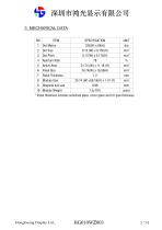
深圳市鸿光显示有限公司 3. MECHANICAL DATA NO Aperture Rate Active Area Panel Size Module Size * Panel thickness includes substrate glass, cover glass and UV glue thickness.
Open the catalog to page 5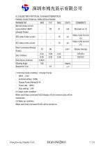
5.2 ELECTRO-OPTICAL CHARACTERISTICS PANEL ELECTRICAL SPECIFICATIONS (1) Normal mode condition: (Charge Pump) - VBAT = 3.6V - Contrast setting : 0XB0 - Charge Pump Setting:0x14 - Frame rate : 105Hz - Duty setting : 1/64 (2) Sleep mode condition: When send 0xae command OLED display off and memory data will be maintained. (3) Wake up condition: When send 0xaf command OLED will be turned on.
Open the catalog to page 7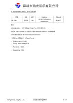
Note: (A) Under VBAT = 3.6V (Charge Pump), Ta = 25°C, 50% RH. (B) Life time is defined the amount of time when the luminance has decayed to less than 50% of the initial measured luminance. (1) Setting of 90cd/m2 : (Charge Pump) - Contrast setting : 0Xb0 - Charge Pump Setting:0x14 - Frame rate : 105Hz - Duty setting : 1/64
Open the catalog to page 8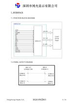
深圳市鸿光显示有限公司 7. INTERFACE 7.1 FUNCTION BLOCK DIAGRAM 7.2 PANEL LAYOUT DIAGRAM
Open the catalog to page 9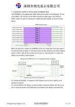
7.4 GRAPHIC DISPLAY DATA RAM ADDRESS MAP The GDDRAM is a bit mapped static RAM holding the bit pattern to be displayed. The size of the RAM is 128 x 64 bits and the RAM is divided into eight pages, from PAGE0 to PAGE7, which are used for monochrome 128x64 dot matrix display, as shown in below figures. GDDRAM pane' structure When one data byte is written into GDDRAM, all the rows image data of the same page of the current column are filled (i.e. the whole column (8 bits) pointed by the column address pointer is filled.). Data bit D0 is written into the top row, while data bit D7 is written into...
Open the catalog to page 12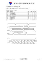
7.5 INTERFACE TIMING CHART 7.5.1 4-Wire Serial Interface Timing Characteristics
Open the catalog to page 13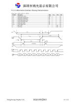
7.5.2 3-Wire Serial Interface Timing Characteristics
Open the catalog to page 14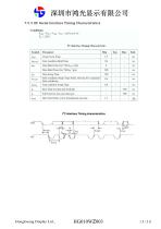
7.5.3 IIC Serial Interface Timing Characteristics Conditions: V’dd * V&s =VDD - V’ss - 1.65V to 3.3 V i'a : PC' Interface Timing Characteristics l2C interface Timing characteristics y^::z:::xjrx kcrno
Open the catalog to page 15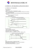
8. POWER ON / OFF SEQUENCE & APPLICATION CIRCUIT8.1 POWER ON / OFF SEQUENCE Power ON sequence: 2. Wait for toN- Power ON Vbat.(1) (where Minimum tow = Oms) 3. After Vdd become stable, wait at least 20ms (to), set RES# pin LOW (logic low) for at least 3us (ti)l3land then HIGH (logic high). 4. After set RES# pin LOW (logic low), wait for at least 3us(tj).Then input commands with below sequence: a. 8Dh for enabling internal charge pump b. AFh for display ON 5. SEG/COM will be ON after 100ms (W). Note: (1 )Vbat should be kept float (i.e. disable) when it is OFF. (2)Power Pins (Vbat) can never be...
Open the catalog to page 16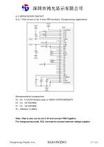
深圳市鸿光显示有限公司 8.2 APPLICATION CIRCUIT 8.2.1 This circuit is for 4 wire SPI interface, Charge pump application. Note: Vbat is also can be set 3.3V and connect VDD together. For charge pump mode, VCC not need to connect external voltage supplier.
Open the catalog to page 17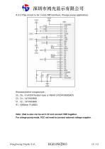
深圳市鸿光显示有限公司 8.2.2 This circuit is for 3 wire SPI interface, Charge pump application. Note: Vbat is also can be set 3.3V and connect VDD together. For charge pump mode, VCC not need to connect external voltage supplier.
Open the catalog to page 18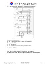
深圳市鸿光显示有限公司 8.2.3 This circuit is for IIC interface, Charge pump application. Recommended components: C5、C6:4.7uF/25V(Tantalum type) or VISHAY (572D475X0025A2T) C3、C4:1uF/16V(0603) C1、C2:1uF/16V(0603) R2、R3:10K(0603) (Should be adjusted based on IIC waveform) R1:620Kohm 1%(0603) Note: Vbat is also can be set 3.3V and connect VDD together. For charge pump mode, VCC not need to connect external voltage supplier.
Open the catalog to page 19
深圳市鸿光显示有限公司 8.3 Initial code void Initial_ic(void) { Write_Command(0xAE); //Display Off Write_Command(0xD5); //SET DISPLAY CLOCK Write_Command(0x90); //105HZ Write_Command(0xA8); //Select Multiplex Ratio Write_Command(0x3F); //Default => 0x3F (1/64 Duty) Write_Command(0xD3); //Setting Display Offset Write_Command(0x00); //00H Reset Write_Command(0x40); //Set Display Start Line Write_Command(0x8D); //Set Charge Pump //Write_Command(0x10); //Disable Charge Pump Write_command(0x14); //Enable Charge Pump Write_command(0xAD); // Internal IREF Setting Write_command(0x20); // Disable internal IREF //Write_command(0x30);...
Open the catalog to page 20
深圳市鸿光显示有限公司 Write_Command(0x30); Write_Command(0xA4); //Entire Display ON Write_Command(0xA6); //Set Normal Display Clear_Ram(); Write_Command(0xAF); //Display ON } void Clear_Ram (void) { int i,j; for(i=0;i<8;i++) { Write_Command (0xb0+i); //Set Page Write_Command (0x00); //Lower Column Address Write_Command (0x10); //Higher Column Address for(j=0;j<128;j++) { data_out(0x00); } } 8.4 COMMAND TABLE Refer to IC Spec.: SSD1315
Open the catalog to page 21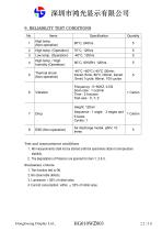
9. RELIABILITY TEST CONDITIONS No. Test and measurement conditions 1. All measurements shall not be started until the specimens attain to temperature stability. 2. The degradation of Polarizer are ignored for item 1,3 & 5. Evaluation criteria 1. The function test is OK. 2. No observable defects. 3. Luminance: > 50% of initial value. 4. Current consumption: within ± 50% of initial value.
Open the catalog to page 22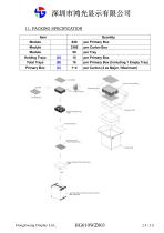
深圳市鸿光显示有限公司 11. PACKING SPECIFICATION Item Holding Trays Total Trays per Primary Box (Including 1 Empty Tray) per Carton (4 as Major / Maximum)
Open the catalog to page 24All Shenzhen Hongguang Display Co., Ltd catalogs and technical brochures
 HG215FH008T01
30 Pages
 HG185FH005
21 Pages
 HG170SX006T01
20 Pages
 HG160WQ004
64 Pages
 HG156FH011
23 Pages
 HG133FH017T01
32 Pages
 HG121WX001T01
22 Pages
 HG116FH008
24 Pages
 HG104SV003
27 Pages
 HG101WX054
12 Pages
 HG101WX053
12 Pages
 HG101WX049
38 Pages
 HG101WX047T01
19 Pages
 HG101WX047
19 Pages
 HG101WX046
18 Pages
 HG101WX030
24 Pages
 HG101WX028
21 Pages
 HG101WX026T01
20 Pages
 HG101WX025
19 Pages
 HG101WX022
19 Pages
 HG101WX021T01
20 Pages
 HG101WX021
20 Pages
 HG050WV038
18 Pages
 HG101WX019T01
20 Pages
 HG101WX019
20 Pages
 HG101WX016
20 Pages
 HG101WX005T01
22 Pages
 HG101WU076
25 Pages
 HG101WU072T01
23 Pages
 HG101WU072
23 Pages
 HG101WU065
23 Pages
 HG101WU063
24 Pages
 HG101WU062
27 Pages
 HG101WU039
30 Pages
 HG101WU035
23 Pages
 HG101WU032T01
18 Pages
 HG101WU013
17 Pages
 HG101WU010
17 Pages
 HG101WU008T01
17 Pages
 HG101WS045
22 Pages
 HG101WS042
17 Pages
 HG101WS040
19 Pages
 HG101WQ004T01
13 Pages
 HG101WQ003
13 Pages
 HG097XG006T01
17 Pages
 HG097QX005
17 Pages
 HG097QX003Z05
18 Pages
 HG097QX003T02
18 Pages
 HG097QX003T01
18 Pages
 HG090WS008
19 Pages
 HG080WX034
19 Pages
 HG080WX032
12 Pages
 HG080WX015
19 Pages
 HG080WX013
19 Pages
 HG080WV029
20 Pages
 HG080WV027
22 Pages
 HG080WU018T01
19 Pages
 HG080WU009
14 Pages
 HG070WX006
13 Pages
 HG070WX005
19 Pages
 HG070WS051T01
19 Pages
 HG070WV048
23 Pages
 HG070WV047
23 Pages
 HG070WV037R01
20 Pages
 HG070WV035T01
19 Pages
 HG070WV035
18 Pages
 HG070WV031
12 Pages
 HG070WV026
23 Pages
 HG070WV022
23 Pages
 HG070WV020
12 Pages
 HG070WV013T01
20 Pages
 HG070WV013R02
20 Pages
 HG070WU039
25 Pages
 HG070WS055
14 Pages
 HG070WS052
13 Pages
 HG070WV051T01
19 Pages
 HG070WS050
22 Pages
 HG070WS049T02
13 Pages
 HG070WS049T01
13 Pages
 HG070WS049-V1
21 Pages
 HG070WS048
25 Pages
 HG070WS046T03
13 Pages
 HG050HD030-V3
18 Pages
 HG215FH008T02
30 Pages
 HG104SV004
21 Pages
 HG050HD030T01
18 Pages
Archived catalogs
 HG043HV026
16 Pages
 HG024QV023R01
1 Page
 HG030FH006T02
16 Pages
 HG055FH018T01
20 Pages
 HG055HD017
16 Pages
 HG055FH021
20 Pages
 HG005WS003
39 Pages
 HG007WS003
50 Pages
 HG015WZ003
49 Pages
 HG080STD02C
7 Pages
 HG104VG002-V0
20 Pages
 HG215FH008
30 Pages
 HG097XG008
17 Pages
 HGYD2690H-V1
21 Pages
 HG173FH002G01
30 Pages
 HG173FH002
30 Pages
 HG043HV002T02
17 Pages
 HG050WV009
19 Pages
 HG028HS003
15 Pages
 HG032WV001
17 Pages
 HG032XG003
19 Pages
 HG034SV004
14 Pages
 HG035SV003
22 Pages
 HG039WV004
19 Pages
 HG040HH005
16 Pages
 HG040HS002T01
16 Pages
 HG040WV006T02
18 Pages
 HG043HV002P01
10 Pages
 HG043HV002R03
17 Pages
 HG043WV005T01
19 Pages
 HG140FH005
20 Pages
 HG043HV008
17 Pages
 HG043HV008T01
17 Pages
 HG043HV009
21 Pages
 HG043HV010
21 Pages
 HG050WV010
19 Pages
 HG030FW006
14 Pages
 HG043HV022
16 Pages
 HG043HV028
20 Pages
 HG043WV016
18 Pages
 HG043WV023T01
19 Pages
 HG043HV029
19 Pages
 HG080WX039-V0
19 Pages
 HG050FH028T02
18 Pages
 HG050HD026T01
18 Pages
 HG101WU042-V0
29 Pages
 HG060HD012
18 Pages
 HG025HV006
12 Pages
 HG050QZ002
21 Pages
 HG050WV005
18 Pages
 HG050WV005T01
18 Pages
 HG050WV008T01
20 Pages
 HG050WV09G01
19 Pages
 HG050WV032
10 Pages
 HG050WV032T01
10 Pages
 HG050WV033
10 Pages
 HG050WV034
20 Pages
 HG055HD016T01
19 Pages
 HG062WV003
19 Pages
 HG062WV006
20 Pages
 HG064XG003
20 Pages
 HG069HS004
20 Pages
 HG070WS004T06
13 Pages
 HG070WS011
13 Pages
 HG070WS012
26 Pages
 HG070WS002
13 Pages
 HG070WS004P01
22 Pages
 HG070WS013
24 Pages
 HG070WS018
19 Pages
 HG070WS045
13 Pages
 HG070WS045T01
13 Pages
 HG070WS045T02
13 Pages
 HG070WS046T02
13 Pages

- LCD display panel
- Industrial display panel
- TFT display module
- Touch screen display panel
- Color display panel
- LED display panel
- Electronic display panel
- Control display system
- IPS display panel
- Programmable display system
- Information display
- RS-232 display panel
- Outdoor display panel
- Built-in display
- Instrumentation display panel
- Medical equipment display
- Control panel display panel
- RGB display panel