- Company
- Products
- Catalogs
- News & Trends
- Exhibitions
HG005WS003
1 /39Pages

HG005WS003
1 /39Pages
Catalog excerpts

SPECIFICATION FOR TFT LCD MODULECUSTOMER:CUSTOMER MODULE :_ HL MODEL : HG005WS003 □Preliminary Specification ■Final Specification Customer Confirmation column: Approved by :Dept. :Data : Please return one of the copies of the specification with your signature to us within two weeks after you receive this document.If it is not returned,we will assume that you agree to the entire contents of this specification document.
Open the catalog to page 1
深圳市鸿光显示有限公司 REVISION RECORD REV. REVISION DESCRIPTION X01 INITIAL RELEASE
Open the catalog to page 2
CONTENTS ITEM
Open the catalog to page 3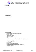
Small molecular organic light emitting diode. Color : White Panel matrix : 48x88 Driver IC : CH1115 Excellent quick response time. Extremely thin thickness for best mechanism design : 1.227 mm High contrast : 10,000:1 Wide viewing angle : 160° I2C interface. Strong environmental resistance. Wide range of operating temperature : -40 to 70° C. Anti-glare polarize
Open the catalog to page 4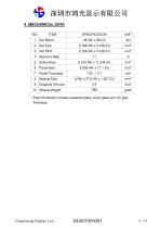
深圳市鸿光显示有限公司 4. MECHANICAL DATA NO Aperture Rate Active Area Panel Size Module Size * Panel thickness includes substrate glass, cover glass and UV glue thickness.
Open the catalog to page 5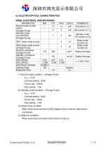
PANEL ELECTRICAL SPECIFICATIONS (1) Normal mode condition : (Charge Pump) ■ V dd2 = 3.3V - Contrast setting : 0x39 ■ Frame rate : 105Hz - Duty setting : 1/48 (2) Standby mode condition : (Charge Pump) - VDD2 = 3.3V - Contrast setting : 0x00 - Frame rate : 105Hz - Duty setting : 1/48 (3) Sleep mode condition : When send 0xae command OLED display off and memory data will be maintained. (4) Wake up condition : When send 0xaf command OLED will be turned on.
Open the catalog to page 7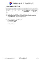
Note: (A) Under Vdd2 = 3.3V (Charge Pump), Ta = 25°C, 50% RH. (B) Life time is defined the amount of time when the luminance has decayed to less than 50% of the initial measured luminance. (1) Setting of 200 cd/m2 : (Charge Pump) - Contrast setting : 0x39 - Frame rate : 105Hz - Duty setting : 1/48
Open the catalog to page 8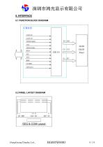
8. INTERFACE 8.1 FUNCTION BLOCK DIAGRAM r----------- vcomh VPP(VCC) 8.2 PANEL LAYOUT DIAGRAM
Open the catalog to page 9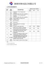
(1) Low is connected to VSS. (2) High is connected to VDD1(VDD).
Open the catalog to page 10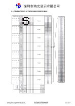
Page Address Line Address
Open the catalog to page 11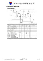
8.5 INTERFACE TIMING CHART l2C interface characteristics
Open the catalog to page 12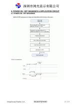
深圳市鸿光显示有限公司 9. POWER ON / OFF SEQUENCE & APPLICATION CIRCUIT 9.1 POWER ON / OFF SEQUENCE
Open the catalog to page 13
深圳市鸿光显示有限公司 9.2 APPLICATION CIRCUIT (Charge Pump) Recommended components: : C1: 4.7uF/16V(0805) C2、C3、C5、C6: 1uF/6.3V(0603) C4: 4.7uF/25V(Tantalum type) or VISHAY (572D475X0025A2T) Riref: 620K ohm 1%(0603) R1、R2: 10K ohm (0603) This circuit is for I2C interface. 9.3 COMMAND TABLE Refer to CH1115 IC Spec.
Open the catalog to page 15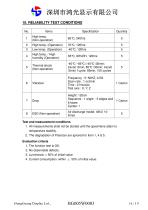
Test and measurement conditions 1. All measurements shall not be started until the specimens attain to temperature stability. 2. The degradation of Polarizer are ignored for item 1,4 & 5. Evaluation criteria 1. The function test is OK. 2. No observable defects. 3. Luminance: > 50% of initial value. 4. Current consumption: within ± 50% of initial value.
Open the catalog to page 16
深圳市鸿光显示有限公司 12. PACKING SPECIFICATION TBD
Open the catalog to page 18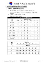
13. OUTGOING INSPECTION PROVISION 1. / SAMPLING METHOD (i) mil-std-1 916 / mrn&m level iii / MIL-STD-1916 / inspection level III / normal inspection / single sample inspection Major Level III ; Minor Level II
Open the catalog to page 19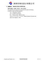
深圳市鸿光显示有限公司 2. 檢驗條件 / INSPECTION CONDITION 檢查和測量在下列條件下進行的,除非另有規定。 檢查和測量在下列條件下進行的,除非另有規定。 The inspection and meaurement are performed under the following conditions, unless otherwise specified. 溫度 / Temperature: 25±5° C 濕度 / Humidity: 50±10%R.H. 壓力 / Pressure: 860~1060
Open the catalog to page 20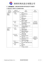
深圳市鸿光显示有限公司 3. 品質檢驗規格 / SPECIFICATION FOR QUALITY CHECK 3.1 缺陷分類 / DEFECT CLASSIFICATION 嚴重度 Severity 主要缺陷 Major Defect 次要缺陷 Minor Defect 檢驗項目 缺陷 Inspection Item Defect 1. 面板 (1) 無顯示 Panel Non-displaying (2) 線缺陷 Line defects (3) 故障 Malfunction (4) 玻璃破損 Glass cracked 2. 軟板 (1) 軟板尺寸超規 Film Film dimension out of specification 3. 尺寸 (1) 外形尺寸超規 Dimension Outline dimension out of specification 1. 面板 (1) 玻璃刮傷 Panel Glass scratch (2) 玻璃切割異常 Glass cutting NG (3) 玻璃崩邊、崩角 Glass chip 2. 偏光板 (1) 偏光板刮傷 Polarizer Polarizer scratch (2) 表面汙漬 Stains on surface (3) 偏光板氣泡 Polarizer bubbles 3. 顯示
Open the catalog to page 21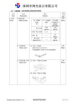
2. mmrn Glass crack Propagation crack is not acceptable. 3. mmm'mrn Glass chip
Open the catalog to page 22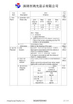
Description wuminin Glass chip ffi£ / Note: 1. t = wuw-M t = glass thickness 2. mmmmnmwm ito ° Chip on the corner extending into the ITO contact is not acceptable. 4. mm Dimension ii. fiBK 1. MM Polarizer Scratch Refer to the drawing of the spec_ Spot type in accordance with the criteria of “Item II-3. Polarizer bubble”. ftBMM “mu i-i wmrnm” ®mm° Line type in accordance with the criteria of “Item I-1. Glass scratch”. Stains cannot be removed even when wiped lightly with a soft cloth or similar cleaning.
Open the catalog to page 23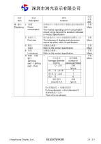
III. 顯示 1. 耗電 Displaying Power consumption 2. 像素尺寸 Pixel size 3. 顏色 Color 4. 亮度 Luminance 5. 暗點、亮點 、 髒污 Dimming spot、Lighting spot、Dust 標準 Criterion 該模組的工作電流消耗不應超出產品規格書的 規範。 The module operating current consumption should not go beyond the standard indicated in Product Specification 顯示像素的尺寸的公差應規格的±25%之內。 The tolerance of display pixel dimension should be within ±25% of specification. 依據產品規格。 Refer to the product specification. 依據產品規格。 Refer to the product specification. 1. 平均直徑 容許個數 Average diameter number of D:(mm) pieces permitted D ≦0.1 忽略 Ignore 1 0.1 ﹤D ≦0.15 0.15﹤D ≦0.2 0.2 ﹤D 顯
Open the catalog to page 24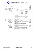
III. 顯示 5. 暗點、亮點 、 2. 寬 Displaying 髒污 width(mm) Dimming W spot 、 Lighting spot、Dust W≦0.03 0.03﹤W≦0.05 0.05﹤W 顯示區外 beyond A.A. IV. 軟板 Film 容許個數 number of pieces permitted 忽略 Ignore 3 無 None 忽略 Ignore 軟板尺寸超規。 Film dimension out of Spec. 破損;深刮傷;深摺痕;深壓痕或其他損害是 不能接受的。 Crack; deep scratch; deep fold; deep pressure mark or other damage is not acceptable. 導電異物附著在導
Open the catalog to page 25
深圳市鸿光显示有限公司 14. APPENDIXES APPENDIX 1: DEFINITIONS A. DEFINITION OF CHROMATICITY COORDINATE The chromaticity coordinate is defined as the coordinate value on the CIE 1931 color chart for R, G, B, W. B. DEFINITION OF CONTRAST RATIO The contrast ratio is defined as the following formula: Luminance of all pixels on measurement Contrast Ratio = Luminance of all pixels off measurement C. DEFINITION OF RESPONSE TIME The definition of turn-on response time Tr is the time interval between a pixel reaching 10% of steady state luminance and 90% of steady state luminance. The definition of turn-off response...
Open the catalog to page 26All Shenzhen Hongguang Display Co., Ltd catalogs and technical brochures
 HG215FH008T01
30 Pages
 HG185FH005
21 Pages
 HG170SX006T01
20 Pages
 HG160WQ004
64 Pages
 HG156FH011
23 Pages
 HG133FH017T01
32 Pages
 HG121WX001T01
22 Pages
 HG116FH008
24 Pages
 HG104SV003
27 Pages
 HG101WX054
12 Pages
 HG101WX053
12 Pages
 HG101WX049
38 Pages
 HG101WX047T01
19 Pages
 HG101WX047
19 Pages
 HG101WX046
18 Pages
 HG101WX030
24 Pages
 HG101WX028
21 Pages
 HG101WX026T01
20 Pages
 HG101WX025
19 Pages
 HG101WX022
19 Pages
 HG101WX021T01
20 Pages
 HG101WX021
20 Pages
 HG050WV038
18 Pages
 HG101WX019T01
20 Pages
 HG101WX019
20 Pages
 HG101WX016
20 Pages
 HG101WX005T01
22 Pages
 HG101WU076
25 Pages
 HG101WU072T01
23 Pages
 HG101WU072
23 Pages
 HG101WU065
23 Pages
 HG101WU063
24 Pages
 HG101WU062
27 Pages
 HG101WU039
30 Pages
 HG101WU035
23 Pages
 HG101WU032T01
18 Pages
 HG101WU013
17 Pages
 HG101WU010
17 Pages
 HG101WU008T01
17 Pages
 HG101WS045
22 Pages
 HG101WS042
17 Pages
 HG101WS040
19 Pages
 HG101WQ004T01
13 Pages
 HG101WQ003
13 Pages
 HG097XG006T01
17 Pages
 HG097QX005
17 Pages
 HG097QX003Z05
18 Pages
 HG097QX003T02
18 Pages
 HG097QX003T01
18 Pages
 HG090WS008
19 Pages
 HG080WX034
19 Pages
 HG080WX032
12 Pages
 HG080WX015
19 Pages
 HG080WX013
19 Pages
 HG080WV029
20 Pages
 HG080WV027
22 Pages
 HG080WU018T01
19 Pages
 HG080WU009
14 Pages
 HG070WX006
13 Pages
 HG070WX005
19 Pages
 HG070WS051T01
19 Pages
 HG070WV048
23 Pages
 HG070WV047
23 Pages
 HG070WV037R01
20 Pages
 HG070WV035T01
19 Pages
 HG070WV035
18 Pages
 HG070WV031
12 Pages
 HG070WV026
23 Pages
 HG070WV022
23 Pages
 HG070WV020
12 Pages
 HG070WV013T01
20 Pages
 HG070WV013R02
20 Pages
 HG070WU039
25 Pages
 HG070WS055
14 Pages
 HG070WS052
13 Pages
 HG070WV051T01
19 Pages
 HG070WS050
22 Pages
 HG070WS049T02
13 Pages
 HG070WS049T01
13 Pages
 HG070WS049-V1
21 Pages
 HG070WS048
25 Pages
 HG070WS046T03
13 Pages
 HG050HD030-V3
18 Pages
 HG215FH008T02
30 Pages
 HG104SV004
21 Pages
 HG050HD030T01
18 Pages
Archived catalogs
 HG043HV026
16 Pages
 HG024QV023R01
1 Page
 HG030FH006T02
16 Pages
 HG055FH018T01
20 Pages
 HG055HD017
16 Pages
 HG055FH021
20 Pages
 HG007WS003
50 Pages
 HG010WZ003
50 Pages
 HG015WZ003
49 Pages
 HG080STD02C
7 Pages
 HG104VG002-V0
20 Pages
 HG215FH008
30 Pages
 HG097XG008
17 Pages
 HGYD2690H-V1
21 Pages
 HG173FH002G01
30 Pages
 HG173FH002
30 Pages
 HG043HV002T02
17 Pages
 HG050WV009
19 Pages
 HG028HS003
15 Pages
 HG032WV001
17 Pages
 HG032XG003
19 Pages
 HG034SV004
14 Pages
 HG035SV003
22 Pages
 HG039WV004
19 Pages
 HG040HH005
16 Pages
 HG040HS002T01
16 Pages
 HG040WV006T02
18 Pages
 HG043HV002P01
10 Pages
 HG043HV002R03
17 Pages
 HG043WV005T01
19 Pages
 HG140FH005
20 Pages
 HG043HV008
17 Pages
 HG043HV008T01
17 Pages
 HG043HV009
21 Pages
 HG043HV010
21 Pages
 HG050WV010
19 Pages
 HG030FW006
14 Pages
 HG043HV022
16 Pages
 HG043HV028
20 Pages
 HG043WV016
18 Pages
 HG043WV023T01
19 Pages
 HG043HV029
19 Pages
 HG080WX039-V0
19 Pages
 HG050FH028T02
18 Pages
 HG050HD026T01
18 Pages
 HG101WU042-V0
29 Pages
 HG060HD012
18 Pages
 HG025HV006
12 Pages
 HG050QZ002
21 Pages
 HG050WV005
18 Pages
 HG050WV005T01
18 Pages
 HG050WV008T01
20 Pages
 HG050WV09G01
19 Pages
 HG050WV032
10 Pages
 HG050WV032T01
10 Pages
 HG050WV033
10 Pages
 HG050WV034
20 Pages
 HG055HD016T01
19 Pages
 HG062WV003
19 Pages
 HG062WV006
20 Pages
 HG064XG003
20 Pages
 HG069HS004
20 Pages
 HG070WS004T06
13 Pages
 HG070WS011
13 Pages
 HG070WS012
26 Pages
 HG070WS002
13 Pages
 HG070WS004P01
22 Pages
 HG070WS013
24 Pages
 HG070WS018
19 Pages
 HG070WS045
13 Pages
 HG070WS045T01
13 Pages
 HG070WS045T02
13 Pages
 HG070WS046T02
13 Pages

- LCD display panel
- Industrial display panel
- TFT display module
- Touch screen display panel
- Color display panel
- LED display panel
- Electronic display panel
- Control display system
- IPS display panel
- Programmable display system
- Information display
- RS-232 display panel
- Outdoor display panel
- Built-in display
- Instrumentation display panel
- Medical equipment display
- Graphic display panel
- Control panel display panel
- RGB display panel