
- Catalogs
- Shenzhen DeepMaterial Technologies Co., Ltd
- Semiconductor Protective Film


- Company
- Products
- Catalogs
- News & Trends
- Exhibitions
Semiconductor Protective Film

Semiconductor Protective Film
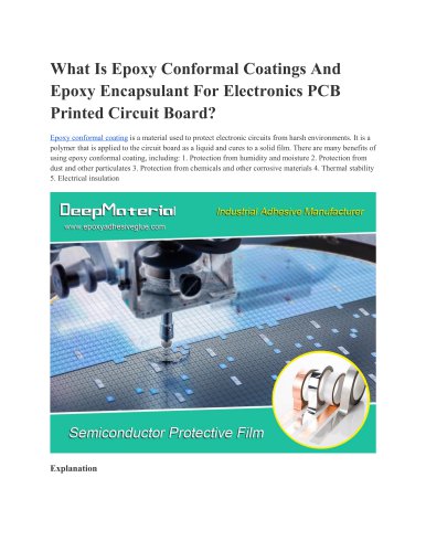
Semiconductor device fabrication involves the deposition of thin films on silicon wafers using vapor deposition, a process that deposits material one atomic layer at a time. As semiconductor devices shrink, precise measurement of these films and their creation conditions becomes crucial. DeepMaterial collaborates with industry partners to enhance thin film deposition monitoring and data analysis, providing improved insights into the systems and chemicals forming these films.
DeepMaterial offers essential measurement and data tools to optimize manufacturing conditions. Their optical system for real-time film growth monitoring offers higher sensitivity than traditional methods, enabling manufacturers to explore new chemical precursors and film interactions, resulting in better film properties.
The company provides a special film using PO as a surface protection material, primarily for QFN cutting, SMD microphone substrate cutting, and FR4 substrate cutting (LED).
DeepMaterial (Shenzhen) Co., Ltd. specializes in adhesives for semiconductor and electronic applications and surface protection materials for chip packaging and testing. They develop adhesives for various applications and protective films, semiconductor fillers, and packaging materials. The company focuses on EB curing adhesives and new semiconductor materials, aiming to overcome technical bottlenecks and achieve breakthroughs in semiconductor protective materials.
Email: [email protected]
Phone: +86-13352636504
Address: 7th Floor, Building C, Comlong Science & Technology Park, Guanlan High-tech Park, Longhua District, Shenzhen, Guangdong, China
Website: www.deepmaterialcn.com
Catalog excerpts

Semiconductor Protective Film Semiconductor device fabrication begins with the deposition of extremely thin films of material on silicon wafers. These films are deposited one atomic layer at a time using a process called vapor deposition. Accurate measurements of these thin films and the conditions used to create them are becoming evermore critical as semiconductor devices such as those found in computer chips shrink. DeepMaterial partnered with chemical suppliers, deposition process tool manufacturers and others in industry to develop an advanced thin film deposition monitoring and data analysis scheme that provides a much-improved view of the systems and chemicals that form these ultrathin films. DeepMaterial provides this industry with essential measurement and data tools that help identify optimal manufacturing conditions. Vapor deposition thin film growth depends on controlled delivery of chemical precursors to the silicon wafer surface. Semiconductor equipment manufacturers use DeepMaterial measurement methods and data analysis to improve their systems for optimal vapor deposition film growth. For example, DeepMaterial developed an optical system that monitors film growth in realtime, with significantly higher sensitivity compared with traditional approaches. With better monitoring systems, semiconductor manufacturers can more confidently explore the use of new chemical precursors and how layers of different films react with each other. The result is better “recipes” for films with the ideal properties
Open the catalog to page 1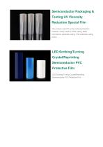
Semiconductor Packaging & Testing UV Viscosity Reduction Special Film The product uses PO as the surface protection material, mainly used for QFN cutting, SMD microphone substrate cutting, FR4 substrate cutting (LED). LED Scribing/Turning Crystal/Reprinting Semiconductor PVC Protective Film LED Scribing/Turning Crystal/Reprinting Semiconductor PVC Protective Film
Open the catalog to page 2
About Us DeepMaterial (Shenzhen) Co., Ltd. is an innovative company specializing in adhesives for semiconductor and electronic applications and surface protection materials for chip packaging and testing. Based on the core technolo- gy of adhesives, DeepMaterial has developed adhesives for chip packaging and testing, circuit board-level adhe-sives, and adhesives for electronic products. Based on adhesives, it has developed protective films, semiconductor fillers, and packaging materials for semiconductor wafer processing and chip packaging and testing. To provide electronic adhesives and thin-film...
Open the catalog to page 3All Shenzhen DeepMaterial Technologies Co., Ltd catalogs and technical brochures
 SMT Epoxy Adhesive
3 Pages
 SMT Epoxy Red Adhesive
3 Pages
 PCB Potting Compound
3 Pages
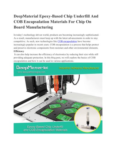 DeepMaterial Epoxy-Based
3 Pages
 BGA Underfill Epoxy
3 Pages
 UV curable adhesive
3 Pages
 UV Conformal Coating
3 Pages
 Underfill Epoxy BGA
3 Pages
 Two component Epoxy Adhesive
4 Pages
 PUR Structural Adhesive
3 Pages
 Epoxy Encapsulant
3 Pages
 Waterproof adhesive glue
4 Pages
 SMT SMD epoxy adhesive
4 Pages
 Optical bonding adhesive
4 Pages
 Hot melt adhesive glue
4 Pages
 Magnet bonding adhesives
4 Pages
 LCD optical bonding adhesive
4 Pages
 Best epoxy adhesie for metal
4 Pages
 UV Curing UV Adhesive
13 Pages
 Structural Bonding Adhesive
10 Pages
 Functional Protective Film
3 Pages









- Single-component adhesive
- Adhesive tape
- Metal adhesive
- Industrial adhesive
- Plastic adhesive
- Glass adhesive
- Dispersion adhesive
- Epoxy adhesive
- Bonding adhesive
- Two-component adhesive
- Ceramic adhesive
- Sealing adhesive
- Fast curing adhesive
- Viscosity adhesive
- Conductivity adhesive
- Wood adhesive
- Packaging foil
- Rubber adhesive