- Catalogs
- Shashin Kagaku
- Compact Film Thickness Monitor
Compact Film Thickness Monitor
1 /2Pages

Compact Film Thickness Monitor
1 /2Pages
Catalog excerpts

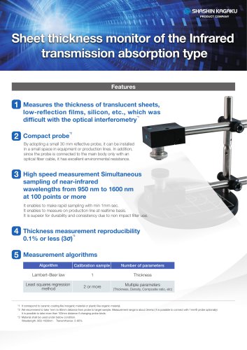
Compact film thickness monitor It corresponds to wide range of application for 10μm to 300μm film thickness Compact probe with the optical fiber can be installed in a small space inside the process tool. Since the 30 mm probe is connected with a optical fiber, it has good durablity. Good repeatability of the film thickness measurement 0.1nm(3σ) Multilayer film thickness measurement up to 9 layers Material analysis function ・ Evaluation of mixing ratio of the composite material using EMA ・ Crystallinity and Analysisy of the optical constants [*5] Selectable light source Light source Target thickness area nm) Typical life time Hour) ( ( Wireless (Option) Film thickness end point detection software is included Automatic mapping stage (Option) Note [*1] It is recommended that the distance from the target surface to the probe is 1mm to 80mm. The measurement area is about 3mmΦ. 1mmΦ pinhole attachement is additionally prepared. Larger probe is available for the long work distance . [*2] The following environment is recommended. 0.1nm(3sigma) SiO2 on Si, Thickness range is 30nm to 1um 0.01%(3sigma) SiO2 on Si, Thickness range is over 1um [*3] The maximum number of layer depends on the actual film structure and wavelength range. [*4] Effective Medium Approximation (EMA) theory and dielectric function are available for material analysis. They become difficult in case of thin film like less than 100nm. [*5] The best light source depends n the target film thickness and required accuracy. [*6] Available on white LED light source. Power is supplied with Li-Ion battery. Data is communicated via Wi-Fi. [*7] Spectral wavelength range depends on light and spectrometer. [*8] It enables to manage up to 450mm wafer. Recommended system requirements Room temperature : 18 to 45 ℃ Long term : < ±2.0℃/24Hours Short term: < ±1.0℃/1Hour
Open the catalog to page 1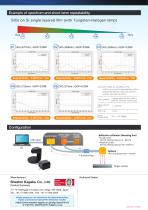
Example of spectrum and short-term repeatability SiO 2 on Si single layered film (with Tungsten-Halogen lamp) Repeatability:0.0036nm(3σ) Note GOF stands for Goodness of Fit, : which is a numerical representation of the fitness between the measured spectrum and the calculated spectrum. Test condition Measurement time 3 sigma when the test wafer is fixed for 30 times continuously Room temperature Configuration Spectrometer USB cable White light source Power supply Reflective collimator (Mounting free) Small probe (3mmΦ, Moving distance 3∼80mm) ● Medium probe (6mmΦ, Moving distance 80∼300mm) ● PC Options...
Open the catalog to page 2All Shashin Kagaku catalogs and technical brochures
 Shashin Kagaku General Brochure
10 Pages
 Kakuhunter Brochure
16 Pages
 SK-400TR
2 Pages
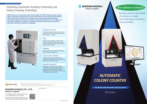 PSF series
4 Pages
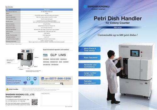 PDH series
2 Pages