- Company
- Products
- Catalogs
- News & Trends
- Exhibitions
SHTW2
1 /14Pages

SHTW2
1 /14Pages
Catalog excerpts

Data Sheet SHTW2 WLCSP Humidity and Temperature Sensor IC Ultra-small flip chip package: 1.3 × 0.7 × 0.5 mm3 Fully calibrated and reflow solderable Ultra-low power consumption Power-up and measurement within 1 ms 1.8 V supply voltage Typical accuracy: ±3 %RH and ±0.3 °C Product Summary The SHTW2 is a digital humidity and temperature sensor in a flip chip package. This type of package opens up a new category of ultra-small humidity sensors which are suitable for applications with the tightest space constraints. At the same time, the flip chip package impresses with its pure simplicity. The sensor is based on Sensirion’s CMOSens® technology, which offers a complete sensor system on a single chip, consisting of a capacitive humidity sensor, a bandgap temperature sensor, analog and digital signal processing, A/D converter, calibration data memory, and a digital communication interface supporting I2C fast mode. Block diagram Benefits of Sensirion’s CMOSens® Technology The sensor covers a humidity measurement range of 0 to 100 %RH and a temperature measurement range of -30 to 100 °C with a typical accuracy of ±3 %RH and ±0.3°C. The operation voltage of 1.8 V and the low power consumption make the SHTW2 suitable for mobile or wireless applications running on the tightest power budgets. With the industry-proven quality and reliability of Sensirion’s humidity and temperature sensors and constant accuracy over a large measurement range, the SHTW2 offers an unprecedented performance-to-price ratio. Tape and reel packaging together with suitability for standard SMD assembly processes make the SHTW2 predestined for high-volume applications. High reliability and long-term stability Industry-proven technology with a track record of more than 10 years Designed for mass production Optimized for lowest cost Best signal-to-noise ratio Signal conditioning Signal conditioning Data processing and system control Calibration mem. VDD Figure 1 Functional block diagram of the
Open the catalog to page 1
1 Humidity and Temperature Sensor SpecificationsRelative Humidity Temperature Table 1 Humidity sensor specifications. Table 2 Temperature sensor specifications. Figure 2 Typical and maximal tolerance for the relative humidity Figure 3 Typical and maximal tolerance for the temperature 1 For definition of typ. and max. accuracy tolerance, please refer to the document “Sensirion Humidity Sensor Specification Statement”. 2 The stated repeatability is 3 times the standard deviation (3a) of multiple consecutive measurement values at constant conditions and is a measure for the noise on the physical...
Open the catalog to page 2
Table 3 Electrical specifications. 2.2 Absolute Maximum Ratings Stress levels beyond those listed in Table 4 may cause permanent damage to the device. These are stress ratings only and functional operation of the device at these conditions cannot be guaranteed. Exposure to the absolute maximum rating conditions for extended periods may affect the reliability of the device. 10 These values can be reduced by using the low power measurement mode, see separate application note.
Open the catalog to page 3
Table 4 Absolute maximum ratings. 3 Timing Specifications 3.1 Sensor System Timings Default conditions of 25 °C and 1.8 V supply voltage apply to values specified in the table below, unless otherwise stated. Max. values are measured at -30°C and 1.98V supply voltage. Table 6 Communication timing specifications. The numbers above are values according to the I2C specification. 11 The recommended storage temperature range is 10-50°C. Please consult the document “SHTxx Handling Instructions ” for more information. 12 These values can be reduced by using the low power measurement mode, see separate...
Open the catalog to page 4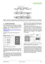
Figure 5 Timing diagram for digital input/output pads. SDA directions are seen from the sensor. Bold SDA lines are controlled by the sensor, plain SDA lines are controlled by the micro-controller. Note that SDA valid read time is triggered by falling edge of preceding toggle. Interface Specifications The SHTW2 supports I2C fast mode (SCL clock frequency from 0 to 400 kHz) with clock stretching. For detailed information on the I2C protocol, refer to NXP I2C-bus specification and user manual UM10204, Rev. 4, February 13, 2012: http://ics.nxp.com/support/documents/interface/pdf/I2C.bu s.specification.pdf...
Open the catalog to page 5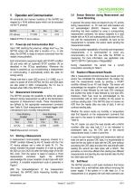
Table 8 SHTW2 I2C device address. Clock Stretching Enabled Table 9 Measurement commands. 5 Operation and Communication All commands and memory locations of the SHTW2 are mapped to a 16-bit address space which can be accessed via the I2C protocol. 5.1 Power-Up and Communication Start Upon VDD reaching the power-up voltage level Vpor, the SHTW2 enters idle state after a duration of tPU. In idle state, the SHTW2 is ready to receive commands from the master (microcontroller). Each transmission sequence begins with START condition (S) and ends with an (optional) STOP condition (P) as described in...
Open the catalog to page 6
Figure 8 Command access communication sequence. The example shows a soft reset command. Clear blocks are controlled by the microcontroller, grey blocks by the SHTW2.
Open the catalog to page 8
6 Quality 6.1 Environmental Stability Qualification of the SHTW2 is performed based on the JEDEC JESD47 qualification test method. 6.2 Material Contents The SHTW2 is RoHS and REACH compliant. 7 Package and Traceability SHTW2 sensors are provided in a flip chip package with an outline of 1.31 x 0.74 x 0.54 mm3 and 4 solder balls with a pitch of 0.4 mm. The humidity sensor is centered on the bottomside of the package. The top side of the package is protected with a black epoxy layer. This is called back side coating, because it is applied to the nonfunctional (back) side of the chip. For a proper...
Open the catalog to page 9
9 Technical Drawings9.1 Package Outline Dim. 9.2 Recommended Metal Land Pattern □ Solder paste dimensions (stencil opening) Figure 11 Recommended metal land pattern for SHTW2 (all dimensions are in mm). Recommended solder paste stencil thickness is 75 to 100 pm. The solder pads on the PCB are recommended to be non solder mask defined (NSMD). Copper traces leading towards the solder pads are recommended to have a width of max. 0.09 mm in the direct vicinity of the pads. For general information on land pattern design refer to the IPC-7351 standard.
Open the catalog to page 10All Sensirion catalogs and technical brochures
 Antifogging Humidity Sensors
2 Pages
 SDP800/810 Digital
14 Pages
 800/810 Analog
8 Pages
 Liquid Flow Meter LG16
8 Pages
 Liquid Flow Meter LG01
4 Pages
 Liquid Flow Meter LS32-1500
4 Pages
 Liquid Flow Meter SLI
8 Pages
 Liquid Flow Meter SLG
7 Pages
 Liquid Flow Meter SLQ-QT105
6 Pages
 Liquid Flow Meter SLQ-QT500
7 Pages
 Liquid Flow Meter SLS-1500
5 Pages
 Liquid Flow Sensor LPG10
5 Pages
 Liquid Flow Sensor LD20
18 Pages
 Temperature Sensor IC STS21
12 Pages
 STS3x-DIS
18 Pages
 Liquid Flow
5 Pages
 Temperature Sensors
4 Pages
 Humidity Sensors
8 Pages
 Antifogging
2 Pages
 Smart Thermostats
2 Pages
 Environmental Sensing
6 Pages
 Datasheet SHTC1
14 Pages
 Datasheet SHT3x digital
21 Pages
 Datasheet SHT3x analog
13 Pages
 LS32-1500
4 Pages
 SHT20
SHT2014 Pages
 Liquid Flow Sensor LG16
5 Pages
 Liquid Flow Sensor LG216
6 Pages


- Flowmeter
- Liquid flow monitor
- Resistance temperature sensor
- Waterproof flow meter
- Gas flow monitor
- Industrial flow monitor
- Pressure probe
- Precision flow meter
- In-line flow meter
- Water flow monitor
- Compact flow monitor
- Gas sensor
- DC flow monitor
- RS485 flow monitor
- Mass flow monitor
- Digital flow monitor
- IP65 flow monitor
- Relative humidity and temperature sensor