- Catalogs
- ON Semiconductor
- 2.5 V / 3.3 V, 106.25 MHz /212.50 MHz PureEdge ™ Dual Frequency LVDS Clock Oscillator Module
2.5 V / 3.3 V, 106.25 MHz /212.50 MHz PureEdge ™ Dual Frequency LVDS Clock Oscillator Module
1 /7Pages

2.5 V / 3.3 V, 106.25 MHz /212.50 MHz PureEdge ™ Dual Frequency LVDS Clock Oscillator Module
1 /7Pages
Catalog excerpts

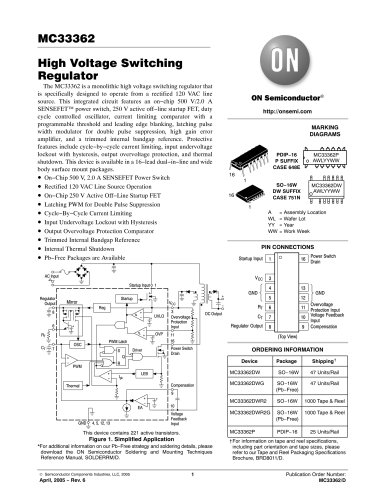
© Semiconductor Components Industries, LLC, 2009 October, 2009 - Rev. 1 1 Publication Order Number: NBXDPA012/D NBXDPA012 2.5 V / 3.3 V, 106.25 MHz / 212.5MHz LVDS Clock Oscillator The NBXDPA012 dual frequency crystal oscillator (XO) is designed to meet today’s requirements for 2.5 V and 3.3 V LVDS clock generation applications. The device uses a high Q fundamental crystal and Phase Lock Loop (PLL) multiplier to provide selectable 106.25 MHz or 212.5 MHz, ultra low jitter and phase noise LVDS differential output. This device is a member of ON Semiconductor’s PureEdge clock family that provides accurate and precision clock solutions. Available in 5 mm x 7 mm SMD (CLCC) package on 16 mm tape and reel in quantities of 1000. Features • LVDS Differential Output • Uses High Q Fundamental Mode Crystal and PLL Multiplier • Ultra Low Jitter and Phase Noise - 0.4 ps (12 kHz - 20 MHz) • Selectable Output Frequency - 106.25 MHz (default) / 212.5 MHz • Hermetically Sealed Ceramic SMD Package • RoHS Compliant • Operating Range: 2.5 V ±5% Operating Range: 3.3 V ±10% • Total Frequency Stability - 50 ppm • This is a Pb-Free Device Applications • 1x and 2x Fiber Channel • Host Bus Adapter Figure 1. Simplified Logic Diagram PLL Clock Multiplier Crystal OE FSEL GND VDD CLK CLK 6 54 1 2 3 http://onsemi.com Device Package Shipping† ORDERING INFORMATION †For information on tape and reel specifications, including part orientation and tape sizes, please refer to our Tape and Reel Packaging Specification Brochure, BRD8011/D. NBXDPA012LN1TAG CLCC-6 (Pb-Free) 1000/ Tape & Reel MARKING DIAGRAM NBXDPA012 = NBXDPA012 (±50 PPM) 106.25/212.5 = Output Frequency (MHz) AA = Assembly Location WL = Wafer Lot YY = Year WW = Work Week G or = Pb-Free Package 6 PIN CLCC LN SUFFIX CASE 848AB NBXDPA012 106.25/212.5 AAWLYYWWG NBXDPA012LNHTAG CLCC-6 (Pb-Free) 100/ Tape & Reel
Open the catalog to page 1
NBXDPA012 http://onsemi.com 2 FSEL OE GND CLK VDD CLK 1 2 3 6 5 4 Figure 2. Pin Connections (Top View) Table 1. PIN DESCRIPTION Pin No. Symbol I/O Description ÁÁÁÁÁ ÁÁÁÁÁ 1 ÁÁÁÁ ÁÁÁÁ OE ÁÁÁÁÁ ÁÁÁÁÁ LVTTL/LVCMOS Control Input ÁÁÁÁÁÁÁÁÁÁÁÁÁÁÁÁÁÁÁÁÁÁ ÁÁÁÁÁÁÁÁÁÁÁÁÁÁÁÁÁÁÁÁÁÁ Output Enable Pin. When left floating pin defaults to logic HIGH and output is active. See OE pin description Table 2. ÁÁÁÁÁ ÁÁÁÁÁ 2 ÁÁÁÁ ÁÁÁÁ FSEL ÁÁÁÁÁ ÁÁÁÁÁ LVTTL/LVCMOS Control Input ÁÁÁÁÁÁÁÁÁÁÁÁÁÁÁÁÁÁÁÁÁÁ ÁÁÁÁÁÁÁÁÁÁÁÁÁÁÁÁÁÁÁÁÁÁ Output Frequency Select Pin. Pin will default to logic HIGH when left open. See Output Frequency...
Open the catalog to page 2
NBXDPA012 http://onsemi.com 3 Table 6. DC CHARACTERISTICS (VDD = 2.5 V ± 5% or VDD = 3.3 V ± 10%, GND = 0 V, TA = -40°C to +85°C) (Note 2) Symbol Characteristic Conditions Min. Typ. Max. Units IDD Power Supply Current 85 105 mA VIH OE and FSEL Input HIGH Voltage 2000 VDD mV VIL OE and FSEL Input LOW Voltage GND - 300 800 mV IIH Input HIGH Current OE FSEL -100 -100 +100 +100 A IIL Input LOW Current OE FSEL -100 -100 +100 +100 A VOD Change in Magnitude of VOD for Complementary Output States (Note 3) 0 1 25 mV VOS Offset Voltage 1125 1375 mV VOS Change in Magnitude of VOS for Complementary Output...
Open the catalog to page 3
NBXDPA012 http://onsemi.com 4 Table 7. AC CHARACTERISTICS (VDD = 2.5 V ± 5% or VDD = 3.3 V ± 10%, GND = 0 V, TA = -40°C to +85°C) (Note 4) Symbol Characteristic Conditions Min. Typ. Max. Units fCLKOUT Output Clock Frequency FSEL = HIGH 106.25 MHz FSEL = LOW 212.5 f Frequency Stability - NBXDPA012 (Note 5) ±50 ppm NOISE Phase-Noise Performance 100 Hz of Carrier -112/-105 dBc/Hz fCLKout = 106.25 MHz/212.5 MHz (See Figures 3 and 4) 1 kHz of Carrier -123/-116 dBc/Hz 10 kHz of Carrier -131/-124 dBc/Hz 100 kHz of Carrier -131/-124 dBc/Hz 1 MHz of Carrier -139/-133 dBc/Hz 10 MHz of Carrier -161/-158...
Open the catalog to page 4
NBXDPA012 http://onsemi.com 5 Figure 3. Typical Phase Noise Plot at 106.25 MHz Figure 4. Typical Phase Noise Plot at 212.5 MHz
Open the catalog to page 5
NBXDPA012 http://onsemi.com 6 Table 8. RELIABILITY COMPLIANCE Parameter Standard Method ÁÁÁÁÁÁÁÁÁÁÁ ÁÁÁÁÁÁÁÁÁÁÁ Shock ÁÁÁÁÁÁÁÁÁÁ ÁÁÁÁÁÁÁÁÁÁ Mechanical ÁÁÁÁÁÁÁÁÁÁÁÁÁÁ ÁÁÁÁÁÁÁÁÁÁÁÁÁÁ MIL-STD-833, Method 2002, Condition B ÁÁÁÁÁÁÁÁÁÁÁ Solderability ÁÁÁÁÁÁÁÁÁÁ Mechanical ÁÁÁÁÁÁÁÁÁÁÁÁÁÁ MIL-STD-833, Method 2003 ÁÁÁÁÁÁÁÁÁÁÁ Vibration ÁÁÁÁÁÁÁÁÁÁ Mechanical ÁÁÁÁÁÁÁÁÁÁÁÁÁÁ MIL-STD-833, Method 2007, Condition A ÁÁÁÁÁÁÁÁÁÁÁ Solvent Resistance ÁÁÁÁÁÁÁÁÁÁ Mechanical ÁÁÁÁÁÁÁÁÁÁÁÁÁÁ MIL-STD-202, Method 215 ÁÁÁÁÁÁÁÁÁÁÁ Resistance to Soldering Heat ÁÁÁÁÁÁÁÁÁÁ Mechanical ÁÁÁÁÁÁÁÁÁÁÁÁÁÁ MIL-STD-203, Method 210,...
Open the catalog to page 6All ON Semiconductor catalogs and technical brochures
 NCV-RSL 15
1 Page
 Networking & Telecom Solutions
28 Pages
 Smart Grid Solutions 2014
16 Pages
 LED Lighting Solutions
48 Pages
 Automotive Products Selector
36 Pages
 White Goods Solutions
32 Pages
 Smart Grid Solutions 2012
12 Pages
 Portable Solutions
28 Pages
 Networking Solutions
24 Pages
 Medical Solutions
16 Pages
 Industrial Solutions
40 Pages
 Image Sensors
12 Pages
 Home Entertainment Solutions
40 Pages
 Computing Solutions
12 Pages
 Automotive Solutions
48 Pages
 1 A Dual H
9 Pages
 Dual 2-Bit Adder / Subtractor
5 Pages
 Quad Analog Switch/Quad Multiplexer
11 Pages


Archived catalogs
 Switching Controllers
20 Pages
 High Power Audio transistors
5 Pages


- Bourn And Koch transceiver
- Motor controller
- Bourn And Koch electronic filter
- Diode
- Potentiometer
- Bourn And Koch transistor
- Stepper motor controller
- Rectifier diode
- Bourn And Koch radio transceiver
- Electronic amplifier
- EMI filter
- SMT diode
- Band-pass electronic filter
- Bourn And Koch bipolar transistor
- Digital motor controller
- Active electronic filter
- Surface-mount oscillator
- Light sensor
- DC drive