- Catalogs
- Scienta Omicron
- Omicron CN 10 V02
Omicron CN 10 V02
1 /2Pages

Omicron CN 10 V02
1 /2Pages
Catalog excerpts
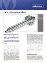
MBE PRO 753-V01/Oct10 CN 10 - Charge Neutraliser The CN 10 is specifically designed to provide charge compensation for analysis of insulating or semiconducting materials during photon or ion bombardment. The CN 10 is an electron source for charge neutralisation. The low energy spread of the BaO filament ensures ultimate XPS resolution on insulators. It is optimised for high beam currents down to lowest energies (10 eV and below). X-ray Photoelectron Spectroscopy (XPS) is ideal for investigating insulating materials such as polymers, ceramics and adhesives etc. However, the XPS technique leads to a depletion of electrons, which are not replaced in insulators, leading to a change in surface potential. The phenomenon of surface charging can be a particular problem during monochromated XPS, where a dynamic equilibrium is not established between the photoelectrons leaving the sample and the electrons delivered from the vacuum or sample bulk. A variable surface charge can cause a decrease in analyser energy resolution due to peak broadening and the shifting of the measured photoelectron peaks. This in turn will reduce the elemental, chemical state and surface www.omicron.de bonding information obtainable from a sample. In order to achieve optimal sensitivity and resolution any surface charging effects must be minimised. The CN 10 is supplied as standard with an activated and tested low work function Barium Oxide emitter, able to supply a current density of up to 400 nAmm2 and a KE of 0 ...16 eV. The creation of an high electron flux allows the operator to selectively tune out varying degrees of localised charging ensuring optimum XPS energy resolution. In addition the CN 10 has been designed to operate as part of a ‘Dual-Beam’ charge neutralisation scheme in combination with the FIG 05 floating ion column. The combination of both ‘slow’ electrons (CN 10) and ions (FIG 05) allows even the most inhomogeneous ceramic compounds to be fully characterised. On samples such as bulk PET FWHM have been measured below 0.71 eV. UHV System integration The CN 10 is available either as part of a fully integrated XPS solution or as a stand-alone unit, flexibly designed for integration into any system with a suitable port. The latest version of
Open the catalog to page 1
the 556 neutraliser control electronics, allow control via the CASCADE experimental control system or as stand-alone software/ manual units. Control via CASCADE allows the user to operate the CN 10 in ‘Dual-Beam’ mode with automatic parameter set-ups for routine and batch sample analysis. Technical Information: Functional outputs Kinetic Energy Range: 0 eV – 16.38 eV with respect to vacuum level Emission Current: 50 µA maximum Target Current: 10 µA with all settings optimised Energy Resolution: 0.8 eV FWHM examining PET C1s peak at 289 eV B.E Focal point / working distance A major benefit of...
Open the catalog to page 2All Scienta Omicron catalogs and technical brochures
 NanoESCA
4 Pages
 UHV Suitcase
2 Pages
 ARPES-Lab
4 Pages
 Cryo Manipulators
2 Pages
 XPS-Lab
2 Pages
 Fermi DryCool SPM
8 Pages
 TESLA JT SPM
8 Pages
 EFM Evaporators
8 Pages
 Argus CU
7 Pages
 UHV NANOPROBE
12 Pages
 Fermi SPM
8 Pages
 Leonova Diamond
8 Pages
 Leonova Emerald
12 Pages
 Intellinova
4 Pages
 MULTIPROBE
8 Pages
 Omicron EFM V05
8 Pages
 PRO-75/100 MBE Systems
2 Pages
 EVO-25/50 MBE Systems
2 Pages
 LAB-10 MBE System
2 Pages
 ISE 5
ISE 52 Pages
 EKF 300
2 Pages
 MBD-LEED
8 Pages
 FOCUS PEEM
16 Pages
 Argus
Argus12 Pages
 MULTISCAN Lab
2 Pages
 LT NANOPROBE
8 Pages
 UHV STM 1
2 Pages
 Cryogenic STM & SFM
4 Pages
 SPHERA
8 Pages
 NanoSAM Lab
6 Pages


Archived catalogs
 VT SPM
11 Pages
 VT SPM_2012
20 Pages
 LT STM_2017
16 Pages
 ESCA+_2010
8 Pages
 LT STM_2012
16 Pages
 MATRIX SPM Control System
8 Pages
 EFM 2
EFM 28 Pages
 CMA 100
4 Pages
 NanoESCA
8 Pages
 SPECTALEED
8 Pages
 SPM PROBE
2 Pages
 EKF 1000
2 Pages
 Multiscan STM
2 Pages
 MS5 & Control Unit
2 Pages
- Liquids analyzer
- Microscope
- Spectrometer
- Integration analyzer
- Laboratory microscope
- Compact analyzer
- Laboratory spectrometer
- Desktop microscope
- Spectrum analyzer
- Process evaporator
- Process spectrometer
- High-resolution spectrometer
- Laboratory evaporator
- Lamp illumination
- Compact illumination
- UV illumination
- Ergonomic microscope
- 3D microscope
- R&D spectrometer
- Modular microscope