- Catalogs
- Scienta Omicron
- NanoESCA
NanoESCA
1 /4Pages

NanoESCA
1 /4Pages
Catalog excerpts

NanoESCA Next-generation photoemission tool for real- and momentum-space microscopy Live View energy-filtered real & momentum space imaging Precise sample spot definition for small area ARPES One-shot 180° ARPES overview without sample movement LHe cooled microscope sample stage and dedicated light-sources Excellent 2D imaging energyresolution (< 25 meV)
Open the catalog to page 1
From microscopy to band-structure mapping Photoemission has a history as one of the leading techniques in material and surface science. In the last decade, 2D k-space imaging or "Momentum Microscopy" has become one of the latest and most promising developments in this field. It allows insight into the electron band-structure of novel material systems, unveiling useful effects that can have a strong impact in future information technology. In combination with real-space imaging it is the ideal tool to make new materials applicable to next-generation devices. B and s tru ctu re is th e k ey to...
Open the catalog to page 2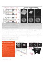
Figure 3: The PEEM column can be easily changed between real-space imaging (a) and momentum-space imaging (b) by adjusting the projection lenses. The electron trajectories of both settngs are equal up to the first imaging plane to allow a reliable positioning of the apertures. The iris-aperture in the first image plane can for example be used to define a small spot on the sample surface (c), from which the momentum-space data can be acquired (d). All shown images were acquired in a 10 s exposure time, the signal being also intense enough for live imaging (500 ms exposure time). The shown images...
Open the catalog to page 3
The combination of a PEEM column with an electrostatic double-hemispherical imaging energy-analyser makes the NanoESCA one of the most promising concepts for surface and material science of the next decade. The 2D mapping of the complete electron momentum distribution at the Fermi level is extremely interesting for novel materials (graphene, topological insulators, TMDs), and will play an important role in the next generation of devices. Engineering functional devices from these new material systems requires easy switching between real- and momentum space, while the live-imaging ability is the...
Open the catalog to page 4All Scienta Omicron catalogs and technical brochures
 UHV Suitcase
2 Pages
 ARPES-Lab
4 Pages
 Cryo Manipulators
2 Pages
 XPS-Lab
2 Pages
 Fermi DryCool SPM
8 Pages
 TESLA JT SPM
8 Pages
 EFM Evaporators
8 Pages
 Argus CU
7 Pages
 UHV NANOPROBE
12 Pages
 Fermi SPM
8 Pages
 Leonova Diamond
8 Pages
 Leonova Emerald
12 Pages
 Intellinova
4 Pages
 MULTIPROBE
8 Pages
 Omicron EFM V05
8 Pages
 PRO-75/100 MBE Systems
2 Pages
 EVO-25/50 MBE Systems
2 Pages
 LAB-10 MBE System
2 Pages
 ISE 5
ISE 52 Pages
 EKF 300
2 Pages
 Omicron CN 10 V02
2 Pages
 MBD-LEED
8 Pages
 FOCUS PEEM
16 Pages
 Argus
Argus12 Pages
 MULTISCAN Lab
2 Pages
 LT NANOPROBE
8 Pages
 UHV STM 1
2 Pages
 Cryogenic STM & SFM
4 Pages
 SPHERA
8 Pages
 NanoSAM Lab
6 Pages


Archived catalogs
 VT SPM
11 Pages
 VT SPM_2012
20 Pages
 LT STM_2017
16 Pages
 ESCA+_2010
8 Pages
 LT STM_2012
16 Pages
 MATRIX SPM Control System
8 Pages
 EFM 2
EFM 28 Pages
 CMA 100
4 Pages
 NanoESCA
8 Pages
 SPECTALEED
8 Pages
 SPM PROBE
2 Pages
 EKF 1000
2 Pages
 Multiscan STM
2 Pages
 MS5 & Control Unit
2 Pages
- Liquids analyzer
- Spectrometer
- Integration analyzer
- Laboratory microscope
- Compact analyzer
- Laboratory spectrometer
- Desktop microscope
- Spectrum analyzer
- Process evaporator
- Process spectrometer
- High-resolution spectrometer
- Laboratory evaporator
- Lamp illumination
- Compact illumination
- UV illumination
- Ergonomic microscope
- 3D microscope
- R&D spectrometer
- Modular microscope