- Catalogs
- Scienta Omicron
- MULTISCAN Lab
MULTISCAN Lab
1 /2Pages

MULTISCAN Lab
1 /2Pages
Catalog excerpts
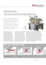
MSLAB 103-V05/10.04 MULTISCAN STM The New Stage for the MULTISCAN LAB™ LAB Increased complexity of today‘s applications requires high-resolution structural and chemical analysis of nanometer-scaled structures. The integral combination of different analysis technologies is the key to gain complementary information of the very same sample area. This goal is ideally achieved with the new goniometermounted MULTISCAN STM, integrated in the MULTISCAN LAB™. To allow optimal and simultaneous SEM and SAM operation together with SPM under different rotation angles, a new scanner design was developed. The SPM ts into the small gap between sample and MULTISCAN LAB™: Complete UHV system solution with UHV Gemini Column and NanoSAM. SEM column with 8 mm working distance. Although the scanner is ultra compact, it offers a scan range of 6 x 6 x 1.5 µm in XYZ, while meeting all stability criteria of a state-of-the-art SPM. Moreover, the rigid design also enables the use of a spring loaded sensor exchange with a non-magnetic tip carrier, avoiding magnetic stray elds for unsurpassed low energy SEM performance. This makes the new MULTISCAN STM an ideal partner for the UHV Gemini Column. The low beam energy performance and ultimate resolution below 3 nm offers unsurpassed SEM capabilities and makes SPM work efciently with SEM assisted probe navigation. Chemical analysis is pushed to previously unknown limits by the introduction of the NanoSAM energy analyser, enabling Scanning Auger Microscopy resolution below the 10 nm benchmark. The new MULTISCAN STM: UHV-Gemini Column NanoSAM EA UHV-Gemini Column NanoSAM EA 8mm MULTISCAN STM Stage UHV-Gemini Column NanoSAM EA 8mm MULTISCAN STM Stage 8mm MULTISCAN STM Stage Side view of the MULTISCAN STM with UHV Gemini The goniometer-mounted MULTISCAN STM with UHV Gemini Column and Column and NanoSAM energy analyser. NanoSAM energy analyser. Schematic with 25° tilted MULTISCAN STM. Omicron NanoTechnology GmbH www.omicron.de 25°
Open the catalog to page 1
:_Nano Technology Atomic resolution STM on Au(111) at Atomic resolution STM on Si(111)- Pre-amplifier technology: Schematic switchable feedback resistors and compensation at the very first operational amplifier stage. (7x7) at a TRUE tunneling current of SEM image of ZnO insulating nanocrystals. Excellent SEM image of Au islands on Carbon. Ultimate resolu- resolution at low beam energy, 200 eV. tion below 3 nm at 15 keV. Line profile showing 2.3 nm resolution. Spot size defined as the 200/o-80°/o width of a step edge. Corresponding silicon line profile with sub- Your local partner: Headquarters:...
Open the catalog to page 2All Scienta Omicron catalogs and technical brochures
 NanoESCA
4 Pages
 UHV Suitcase
2 Pages
 ARPES-Lab
4 Pages
 Cryo Manipulators
2 Pages
 XPS-Lab
2 Pages
 Fermi DryCool SPM
8 Pages
 TESLA JT SPM
8 Pages
 EFM Evaporators
8 Pages
 Argus CU
7 Pages
 UHV NANOPROBE
12 Pages
 Fermi SPM
8 Pages
 Leonova Diamond
8 Pages
 Leonova Emerald
12 Pages
 Intellinova
4 Pages
 MULTIPROBE
8 Pages
 Omicron EFM V05
8 Pages
 PRO-75/100 MBE Systems
2 Pages
 EVO-25/50 MBE Systems
2 Pages
 LAB-10 MBE System
2 Pages
 ISE 5
ISE 52 Pages
 EKF 300
2 Pages
 Omicron CN 10 V02
2 Pages
 MBD-LEED
8 Pages
 FOCUS PEEM
16 Pages
 Argus
Argus12 Pages
 LT NANOPROBE
8 Pages
 UHV STM 1
2 Pages
 Cryogenic STM & SFM
4 Pages
 SPHERA
8 Pages
 NanoSAM Lab
6 Pages


Archived catalogs
 VT SPM
11 Pages
 VT SPM_2012
20 Pages
 LT STM_2017
16 Pages
 ESCA+_2010
8 Pages
 LT STM_2012
16 Pages
 MATRIX SPM Control System
8 Pages
 EFM 2
EFM 28 Pages
 CMA 100
4 Pages
 NanoESCA
8 Pages
 SPECTALEED
8 Pages
 SPM PROBE
2 Pages
 EKF 1000
2 Pages
 Multiscan STM
2 Pages
 MS5 & Control Unit
2 Pages
- Liquids analyzer
- Microscope
- Spectrometer
- Integration analyzer
- Laboratory microscope
- Compact analyzer
- Laboratory spectrometer
- Desktop microscope
- Spectrum analyzer
- Process evaporator
- Process spectrometer
- High-resolution spectrometer
- Laboratory evaporator
- Lamp illumination
- Compact illumination
- UV illumination
- Ergonomic microscope
- 3D microscope
- R&D spectrometer
- Modular microscope