- Catalogs
- Scienta Omicron
- LT NANOPROBE
LT NANOPROBE
1 /8Pages

LT NANOPROBE
1 /8Pages
Catalog excerpts

Ultimate Probing at the Nanoscale • Four Fully Independent Scanning Tunnelling Microscopes • Excellent STM Performance for Spectroscopy and Manipulation • High Resolution SEM Navigation
Open the catalog to page 1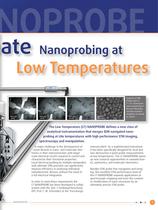
mate Nanoprobing at Low Temperatures 500 µm 500 µm 500 µm 200 nm Sequence of SEM images taken at T < 5 K, showing the coarse positioning of the four STM probes and high resolution imaging on Au islands on carbon. The Low Temperature (LT) NANOPROBE defines a new class of analytical instrumentation that merges SEM navigated nanoprobing at LHe temperatures with high performance STM imaging, spectroscopy and manipulation. A major challenge in the development of novel devices in nano- and molecular electronics is their interconnection with larger scale electrical circuits required to control and characterize...
Open the catalog to page 3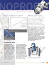
The low beam energy performance of the UHV Gemini Column minimises damage to sensitive samples and enables imaging of nearly insulating samples by minimising charging effects at energies in the few keV range. 4-point electrical transport measurement at T < 5 K. Wires with a width of 1 pm exhibit linear transport behavior. Curves have been taken at different distances between the inner electrodes. SEM imaging parameters: EKIN = 5.00 kV, H. Marbach, Univ. of Erlangen (Germany). For the navigation of four independent STM probes, simultaneous SEM imaging is indis- pensable to bridge dimensions from...
Open the catalog to page 5
Technical Details SPM 1 SPM 4 UHV Gemini column SPM 2 SPM 3 Bath cryostat and thermal shielding in the LT NANOPROBE LHe bath cryostat with T < 5K LN2 cooling Principle schematic showing the LT NANOPROBE cooling. 4 Independent SPM's Cooling Down to T < 5K Magnetic Field The microscope stage carries four individual SPM modules with independent and guided 3D coarse positioning of XYZ = 5x5x3 mm. The sample can be independently positioned by XY = 4x4 mm. Omicron´s patented piezo-electric inertia drives provide highly reliable and efficient navigation with step sizes from a few tens of nm´s up to...
Open the catalog to page 6
+ dI/dU [a.u.] UGap STS on Au(111) using a Nb tip at T < 5 K reveales the superconducting gap of Nb with approx. 3 meV width. IT - + - -+ ++ UGap UGap UGap UGap Parameters: fMOD = 540 Hz, UMOD = 140 µV, TSi-diode = 4.8 K. Deviations from BCS curve shape -8 UGap UGap UGap -6 -4 -2 0 2 UGap [mV] 4 6 8 are due to tip contamination and related tunnelling processes (no tip preparation applied). < 2 pm noise II ITTT 15.0 ≈ 6 pm corrugation 10.0 Height [pm] - -+ ++ 3.0 mV 5.0 0 -5.0 -10.0 -15.0 0 2.5 5.0 7.5 10.0 12.5 Position [nm] 15.0 17.5 20.0 The schematic is showing the function principle of signal...
Open the catalog to page 7
Headquarters: Omicron NanoTechnology GmbH Limburger Str. 75 65232 Taunusstein, Germany Tel. +49 (0) 61 28 / 987 - 0 Fax +49 (0) 61 28 / 987 - 185 Web: www.omicron.de e-mail: [email protected] Minneapolis Pittsburgh East Grinstead Linköping Moscow Poznan Beijing We have agents and partners worldwide – please check our website to find your nearest contact. Seoul Tokyo Taipei Mumbai Omicron NanoTechnology is part of the Oxford Instruments Group. For more information: www.oxford-instruments.com or just send us an e-mail: [email protected] LT NANOPROBE 541-V03/Mar12 Printed by Druckerei und Verlag...
Open the catalog to page 8All Scienta Omicron catalogs and technical brochures
 NanoESCA
4 Pages
 UHV Suitcase
2 Pages
 ARPES-Lab
4 Pages
 Cryo Manipulators
2 Pages
 XPS-Lab
2 Pages
 Fermi DryCool SPM
8 Pages
 TESLA JT SPM
8 Pages
 EFM Evaporators
8 Pages
 Argus CU
7 Pages
 UHV NANOPROBE
12 Pages
 Fermi SPM
8 Pages
 Leonova Diamond
8 Pages
 Leonova Emerald
12 Pages
 Intellinova
4 Pages
 MULTIPROBE
8 Pages
 Omicron EFM V05
8 Pages
 PRO-75/100 MBE Systems
2 Pages
 EVO-25/50 MBE Systems
2 Pages
 LAB-10 MBE System
2 Pages
 ISE 5
ISE 52 Pages
 EKF 300
2 Pages
 Omicron CN 10 V02
2 Pages
 MBD-LEED
8 Pages
 FOCUS PEEM
16 Pages
 Argus
Argus12 Pages
 MULTISCAN Lab
2 Pages
 UHV STM 1
2 Pages
 Cryogenic STM & SFM
4 Pages
 SPHERA
8 Pages
 NanoSAM Lab
6 Pages


Archived catalogs
 VT SPM
11 Pages
 VT SPM_2012
20 Pages
 LT STM_2017
16 Pages
 ESCA+_2010
8 Pages
 LT STM_2012
16 Pages
 MATRIX SPM Control System
8 Pages
 EFM 2
EFM 28 Pages
 CMA 100
4 Pages
 NanoESCA
8 Pages
 SPECTALEED
8 Pages
 SPM PROBE
2 Pages
 EKF 1000
2 Pages
 Multiscan STM
2 Pages
 MS5 & Control Unit
2 Pages
- Liquids analyzer
- Spectrometer
- Integration analyzer
- Laboratory microscope
- Compact analyzer
- Laboratory spectrometer
- Desktop microscope
- Spectrum analyzer
- Process evaporator
- Process spectrometer
- High-resolution spectrometer
- Laboratory evaporator
- Lamp illumination
- Compact illumination
- UV illumination
- Ergonomic microscope
- 3D microscope
- R&D spectrometer
- Modular microscope