
Catalog excerpts

Glass Wafer
Open the catalog to page 1
SCHOTT is an international technology group with more than 125 years of experience in the areas of specialty glasses, materials and advanced technologies. With our high-quality products and intelligent solutions, we contribute to our customers’ success and make SCHOTT part of everyone’s life. SCHOTT Advanced Optics, with its deep technological expertise, is a valuable partner for its customers in developing products and customized solutions for applications in optics, lithography, astronomy, opto-electronics, life sciences, and research. With a product portfolio of more than 100 optical...
Open the catalog to page 2
Unique Wafer Portfolio with Solutions for Your pplications A As “Your Partner for Excellence in Optics” Advanced Optics holds very close relationship with its customers and develops solutions and products reflecting the market’ needs. This is a reason why SCHOTT is today the world’s leading supplier of thin and ultra thin glass wafers made of different materials in sizes between 4” and 12” with different surface qualities and customized features. Applying proprietary production processes, leveraging a selection of different materials and the continuous expansion of s tate-of-the-art...
Open the catalog to page 3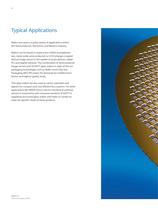
Typical Applications Wafers are used in a great variety of applications within the Semiconductor, Electronics and Biotech industry. Wafers can be found in nearly every CMOS (complementary metal oxide semiconductor) or CCD (charges coupled device) image sensor in the market of smart phones, tablet PCs and digital cameras. The combination of semiconductor image sensors and SCHOTT glass wafers in state-of-the-art packaging technologies such as Wafer Level Chip Size Packaging (WLCSP) meets the demands for smallest form factors and highest quality levels. Thin glass wafers are also used as...
Open the catalog to page 4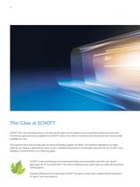
Thin Glass at SCHOTT SCHOTT has a long standing history in producing thin glass and developed various proprietary production processes. The thinnest glass substrates available from SCHOTT are less than 50 µm in thickness and will soon be even commercially available on a reel. This expertise forms the principle pillar for being the leading supplier for Wafers. The relevant materials for our waferofferings are made in a special down-draw process. Detailed characteristics of these glass types (AF 32® eco, D 263® T eco, MEMpax®) are presented on the following pages. SCHOTT is also contributing...
Open the catalog to page 6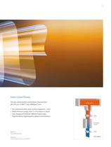
Down-Draw Process The key characteristics of the down-draw process (AF 32® eco, D 263® T eco, MEMpax®) are: Fire-polished surface with surface roughness < 1 m n Wide thickness range, from 1.1 mm down to 25 µm • Fast changeover between different glass types • igh flexibility regarding throughput and thickness H Molten glass Annealing furnace Figure 3 Thin glass (50 μm) Figure 4 Down-Draw process at SCHOTT Glass ribbon
Open the catalog to page 7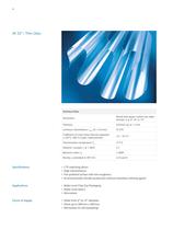
Technical Data Dimensions Round and square custom size wafer formats, e. g. 6“, 8“ or 12“ Coefficient of mean linear thermal expansion α (20 °C; 300 °C) (static measurement) CTE matching silicon • High transmittance • ire-polished surface with low roughness F • nvironmentally friendly production without hazardous refining agents E Wafer Level Chip Size Packaging • Wafer Level Optics • Microsheet Wafer from 4“ to 12“ diameter Sheet up to 300 mm x 300 mm • Microsheet on reel (sampling) •
Open the catalog to page 8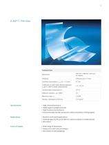
Technical Data Dimensions 440 mm x 360 mm, other size on request Coefficient of mean linear thermal expansion α (20 °C; 300 °C) (static measurement) High chemical resistance • Stable against sunlight and heat • High luminous transmittance • nvironmentally friendly production without hazardous refining agents E Resistive touch panel applications • ubstrate glass for IR cut-off filter for camera modules in mobile phones S • Microsheet Wide range of thicknesses • Variety of in-stock sizes and shapes Microsheet on reel (sampling)
Open the catalog to page 9
Figure 5 Structured wafer for sensor application
Open the catalog to page 10
Technical Data Coefficient of mean linear thermal expansion ^ -j Q-& Specifications • Fire-polished surface • High thermal stability • Enabling anodic bonding with silicon wafers • Excellent transmission • Physical and chemical properties identical with Borofloat* 33 Applications • MEMS • Wafer level packaging • Optical sensors • Lighting solutions Forms of Supply • 6", 8" or 12" wafer
Open the catalog to page 11
Figure 6 Structured glass wafer
Open the catalog to page 12
Main Competences in Glass Wafer Processing Besides offering wafers made of different materials and different sizes SCHOTT has built up extensive experiences and know-how in glass processing. Learning from a SCHOTT history of glass melting and processing of more than 125 years and leveraging a strong network with experts and partners SCHOTT is able to offer wafers in almost any customized structure, surface quality and with individual features. This makes our products unique! Here you find an overview, details of our competencies are gives on the following pages. Process capabilities Cutting...
Open the catalog to page 13
Our Competencies in Detail Polishing With our state-of-art polishing operations and long experience in polishing of thin glass, we can meet and exceed all industry standards and customer requirements. Properties Fire polishing Standard polishing Advanced polishing Edge grinding C-shape Facet C-shape Facet Flatness (warp) Surface defects (Scratch / Digs) according to MIL-PRF 13830B Table 1 Options for polishing Figure 7 Sonotrode Figure 8 Structured substrate With the Powder blasting technology and the Ultrasonic lapping process SCHOTT has established a variety of capabilities to provide...
Open the catalog to page 14
Ultrasonic lapping Size Thickness range Different hole configurations Round holes Round, rectangular holes and caverns Positioning tolerances Table 2 Process capabilities Powder blasting * Tighter tolerances on request Edge Treatment Our expertise in edge treatment offers the choice between flat and notch orientation marking according SEMI industry standards. Wafer edges can be processed to C-shape or facet shape. Options for edge processing Facet Shape
Open the catalog to page 15All SCHOTT GLAS catalogs and technical brochures
-
 SEFUSE® D6S Battery Fuses
2 Pages
-
 SCHOTT PTR70 brochure
12 Pages
-
 Automotive Electronics Brochure
12 Pages
-
 EP Image brochure
32 Pages
-
 Prisms
1 Pages
-
 Polarizers
1 Pages
-
 Optical Components
2 Pages
-
 MEMpax®
1 Pages
-
 Laser Windows
1 Pages
-
 Laser Mirrors
1 Pages
-
 Interference Filters
1 Pages
-
 D 263® T eco Thin Glass
1 Pages
-
 Cylindrical Lenses
1 Pages
-
 Ball Lenses
1 Pages
-
 B 270® & B 270® i Flat Glass
1 Pages
-
 Aspherical Lenses
1 Pages
-
 AF 32® eco Thin Glass
1 Pages
-
 Advanced Optics at a Glance
2 Pages
-
 Optical Filters 2013 - Catalogue
149 Pages
-
 Optical Glass 2011 - Catalogue
114 Pages
-
 ZERODUR
24 Pages
-
 Radiation Shielding Glass
2 Pages
-
 Polished Prism
1 Pages
-
 Optical Glass Coatings
1 Pages
-
 Fused Silica
9 Pages
-
 Optical Glass Catalogue 2010
90 Pages
-
 Glass Filter Catalogue
43 Pages
-
 ZERODUR® Catalogue
22 Pages


