RM40N10PK
1 /5Pages

RM40N10PK
1 /5Pages
Catalog excerpts
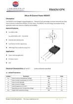
RM40N10PK Silicon N‐Channel Power MOSFET Description This MOSFETs from Rongtech Industry(ShangHai) Inc., Advanced 6 inch technology to achieve extremely low Static Drain‐to‐Source on‐Resistance RDS(on). For this reason, This MOSFETs has low energy consumption during application which also enhances reliability and durability. Extended Safe Operating Area Low Reverse transfer capacitances 100% Single Pulse avalanche energy Test Power switching application Electrical Characteristics @ Ta=25℃ (unless otherwise specified) a) Limited Parameters: Symbol VDSS ID IDM VGS Ptot Tj Eas Parameter Drain‐to‐Source Breakdown Voltage Drain Current (continuous) at Tc=25℃ Drain Current (pulsed) Gate to Source Voltage Total Dissipation at Tc=25℃ Operating Junction Temperature Range Single Pulse Avalanche Energy Rongtech Industry(ShangHai
Open the catalog to page 1
RM40N10PK b) Electrical Parameters: Symbol Parameter VDS Drain‐source Voltage RDS(on) Static Drain‐to‐Source on‐Resistance VGS(th) Gated Threshold Voltage IDSS IGSS(F) IGSS(R) Ciss Coss Crss Qg Qgs Qgd Zero Gate Voltage Drain Current Gated Body Leakage Current Gated Body Leakage Current Input Capacitance Output Capacitance Reverse Transfer Capacitance Total Gate Charge Gate‐Source Charge Gate‐Drain Charge Symbol Parameter td(on) Turn‐on Delay Time tr Turn‐on Rise Time Turn‐off Delay Time Turn‐off Fall Time Symbol Parameter ISD S‐D Current(Body Diode) Test Conditions Pulsed S‐D Current(Body Diode)...
Open the catalog to page 2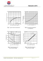
R DS(on) , Drain-to-Source O (Normalized) VGS = 0V, f = 1MHz GS Ciss = Cgs + Cgd , Cds SHORTED Crss = Cgd Coss = Cds + Cgd Fig 3. Typical Capacitance Vs. Drain-to-Source Voltage Rongtech Industry(ShangHai)Inc., Http://www.rongtechpower.com Fig 2. Normalized On-Resistance Vs. Temperature Fig 1. Typical Transfer Characteristics QG , Total Gate Charge (nC) Fig 4. Typical Gate Charge Vs. Gate-to-Source Voltage
Open the catalog to page 3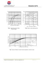
1000 OPERATION IN THIS AREA L LIMITED BY RDS(on) ISD , Reverse Drain Current (A) Fig 6. Maximum Safe Operating Area Fig 5. Typical Source-Drain Diode Forward Voltage Thermal Response (Z thJC) SINGLE PULSE (THERMAL RESPONSE) Notes: 1. Duty factor D = t 1 / 2 2. Peak TJ = P DM x thJC + TC t1 , Rectangular Pulse Duration (sec) Fig 7. Maximum Effective Transient Thermal Impedance, Junction-to-Case Rongtech Industry(ShangHai)Inc., Http://www.rongtechpower.com
Open the catalog to page 4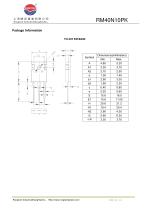
RM40N10PK Package Information TO‐247 PACKAGE Rongtech Industry(ShangHai)Inc., Http://www.rongtechpower.com
Open the catalog to page 5All Rongtech Industry (Shanghai) Inc., catalogs and technical brochures
 RTO600/800/1000AS52 series
3 Pages
 RM110N06PK
5 Pages
 RM110N06PA
5 Pages
 RM75N08PA
5 Pages
 RM70N06PA
5 Pages
 RM60N10PA
5 Pages
 RM50N06PA
5 Pages
 RM45N06PA
5 Pages
 RM40N10PA
5 Pages
 RM30N20PK
5 Pages
 RM20N10PA
5 Pages
 RVS47N60PN
11 Pages
 RTU400SG120FA2
7 Pages
 RTU600SG120FA2
7 Pages
 RTU300HF120FA2
7 Pages
 RTU200HF120FA2
7 Pages
 RTU150HF120FA2
7 Pages
 RTU100HF120FA1
7 Pages
 RTU75HF120FA1
7 Pages
 RTU50HF120FA1
7 Pages
 RTU40HF120FA1
7 Pages
 RTK600SG120B
7 Pages
 RTK400SG120B
7 Pages
 RTK300HF120B
7 Pages
 RTK200HF120B
7 Pages
 "RT25PI120B9H" IGBT Module
13 Pages
 RFR60F30APN
3 Pages
 RFR30F60PN
3 Pages
 RFR30F40PN
3 Pages
 RFM200CC4A2D
3 Pages
 RTVSM100 series
3 Pages
 RTVS4000 series
2 Pages
 RTV25-1000 series
2 Pages
 RTV025A series
2 Pages
 RTO20000HB series
2 Pages
 RTO5000HAX series
2 Pages
 RTO3000HT
2 Pages
 RTO2000K series
2 Pages
 RT0300LB series
2 Pages
 RTO200G3 series
2 Pages
 RTO1000DHR series
2 Pages
 RTO800,1200,1500BHS52 series
3 Pages
 RTO900HC5F series
3 Pages
 RTO600/800/900TF512 series
2 Pages
 RTO500K1 series
2 Pages
 RTO500E series
2 Pages
 RTO600B series
2 Pages
 RTNT1000-C3 series
2 Pages
 RTLT1000/2000SH series
2 Pages
 RTLT1000SH series
2 Pages
 RTC500LTB series
2 Pages
 RTC300TAH series
2 Pages
 RTC100LTA
2 Pages
 RTC200P3
2 Pages
 RTC200LP series
2 Pages
 RTC50LA2
2 Pages
 RTC50Q58 series
2 Pages
 RTC200ECH Series
2 Pages
 RTC100LAH sereies
2 Pages
 RTC50LSRTC50LS
2 Pages
 RTC035A series
2 Pages
 RTC25DT52
2 Pages
 RT40PI120T5H PIM module
10 Pages
 RT25PI120B9H PIM module
11 Pages
 RT10PI120B3H PIM module
7 Pages
 RTM800FF65HP2S IGBT module
10 Pages
 RTR600HF170T9H IGBT module
8 Pages
 RTS600HF120T9H IGBT Module
8 Pages
 RTM400FF120B8S IGBT Module
10 Pages
 RTM400FF75A8H IGBT Module
9 Pages
 RT100PI120T6H-M IGBT module
14 Pages
 RTV25-1000 voltage sensor
2 Pages
 RTV025A voltage sensor
2 Pages
 RTLT1000SH current sensor
2 Pages
 RTNT400-S current sensor
2 Pages
 RTC200ECH current sensor
2 Pages
 RTC100LAH current sensor
2 Pages
 RTC75LX current sensor
2 Pages
 RTC050A current sensor
2 Pages
 RH701 current IC senser
41 Pages
 RTC050DT52 current sensor
2 Pages
 RTC050H5 SERIES
2 Pages
 GT300HF120T2VH IGBT module
6 Pages


Archived catalogs
 RTC06H5
3 Pages
 GT100FF120T6H IGBT module
7 Pages
 GT100HF120T1VH IGBT module
7 Pages


- Power supply unit
- DC power supply
- AC/DC power supply
- Capacitor
- Battery charger
- Current sensor
- Single-phase power supply
- Lead battery charger
- AC current sensor
- Ceramic capacitor
- Transistor module
- DC current sensor
- Automatic battery charger
- SMD capacitor
- Power capacitor
- Lead-acid battery charger
- Mobile battery charger
- Film capacitor
- Rectifier diode