- Catalogs
- ROHM Semiconductor
- RGW60TS65CHR
RGW60TS65CHR
1 /15Pages

RGW60TS65CHR
1 /15Pages
Catalog excerpts
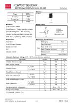
650V 30A Hybrid IGBT with Built-In SiC-SBD lOutline lInner Circuit (1) Gate (2) Collector (3) Emitter 2) Low Collector - Emitter Saturation Voltage *1 3) Low Switching Loss & Soft Switching 4) Built in No Recovery Silicon Carbide SBD 5) Pb - free Lead Plating ; RoHS Compliant lApplication lPackaging Specifications DC-DC Converters Packing Code Industrial Inverter Basic Ordering Unit (pcs) lAbsolute Maximum Ratings (at TC = 25°C unless otherwise specified) Parameter Collector - Emitter Voltage Gate - Emitter Voltage Collector Current Pulsed Collector Current Diode Forward Current Diode Pulsed Forward Current Power Dissipation Operating Junction Temperature Storage Temperature *1 Pulse width limited by Tjmax. www.rohm.com © 2021 ROHM Co., Ltd. All rights reserved.
Open the catalog to page 1
RGW60TS65CHR lThermal Resistance Parameter Thermal Resistance IGBT Junction - Case Thermal Resistance Diode Junction - Case lIGBT Electrical Characteristics (at Tj = 25°C unless otherwise specified) Parameter Collector - Emitter Breakdown Voltage Gate - Emitter Leakage Current Gate - Emitter Threshold Voltage Collector - Emitter Saturation Voltage www.rohm.com © 2021 ROHM Co., Ltd. All rights reserved.
Open the catalog to page 2
RGW60TS65CHR lIGBT Electrical Characteristics (at Tj = 25°C unless otherwise specified) Parameter Input Capacitance Output Capacitance Reverse transfer Capacitance Total Gate Charge Gate - Emitter Charge Gate - Collector Charge Turn - on Delay Time Rise Time Turn - off Delay Time Fall Time Turn - on Switching Loss Turn - off Switching Loss Turn - on Delay Time IC = 15A, VCC = 400V, VGE = 15V, RG = 10Ω, Tj = 25°C Inductive Load *Eon include diode reverse recovery Rise Time Turn - off Delay Time Fall Time Turn - on Switching Loss Turn - off Switching Loss IC = 15A, VCC = 400V, VGE = 15V, RG = 10Ω,...
Open the catalog to page 3
RGW60TS65CHR lSiC-SBD Electrical Characteristics (at Tj = 25°C unless otherwise specified) Parameter IF = 20A, Diode Forward Voltage Diode Reverse Recovery Time Diode Peak Reverse Recovery Current Diode Reverse Recovery Charge Diode Reverse Recovery Energy Diode Reverse Recovery Time Diode Peak Reverse Recovery Current Diode Reverse Recovery Charge Diode Reverse Recovery Energy Total Capacitance www.rohm.com © 2021 ROHM Co., Ltd. All rights reserved.
Open the catalog to page 4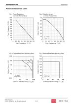
RGW60TS65CHR lElectrical Characteristic Curves Fig.1 Power Dissipation vs. Case Temperature 200 Fig.2 Collector Current vs. Case Temperature 70 60 Fig.3 Forward Bias Safe Operating Area Fig.4 Reverse Bias Safe Operating Area 160 Collector To Emitter Voltage : VCE [V] www.rohm.com © 2021 ROHM Co., Ltd. All rights reserved. Collector To Emitter Voltage : VCE [V]
Open the catalog to page 5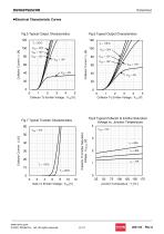
RGW60TS65CHR lElectrical Characteristic Curves Fig.5 Typical Output Characteristics Fig.6 Typical Output Characteristics Collector To Emitter Voltage : VCE [V] Collector To Emitter Saturation Voltage : VCE(sat) [V] Fig.8 Typical Collector to Emitter Saturation Voltage vs. Junction Temperature 4 Fig.7 Typical Transfer Characteristics Collector To Emitter Voltage : VCE [V] Gate To Emitter Voltage : VGE [V] www.rohm.com © 2021 ROHM Co., Ltd. All rights reserved.
Open the catalog to page 6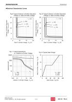
RGW60TS65CHR lElectrical Characteristic Curves Fig.9 Typical Collector to Emitter Saturation Voltage vs. Gate to Emitter Voltage 20 Fig.10 Typical Collector to Emitter Saturation Voltage vs. Gate to Emitter Voltage 20 Tj = 175ºC Collector To Emitter Saturation Voltage : VCE(sat) [V] Collector To Emitter Saturation Voltage : VCE(sat) [V] Gate To Emitter Voltage : VGE [V] Fig.12 Typical Gate Charge 15 Gate To Emitter Voltage : V GE [V] Gate To Emitter Voltage : VGE [V] Fig.11 Typical Capacitance vs. Collector to Emitter Voltage 10000 Cies Collector To Emitter Voltage : VCE [V] www.rohm.com © 2021...
Open the catalog to page 7
RGW60TS65CHR lElectrical Characteristic Curves Fig.13 Typical Switching Time vs. Collector Current 1000 Fig.14 Typical Switching Time vs. Gate Resistance 1000 Fig.16 Typocal Switching Energy Losses vs. Gate Resistance 10 Switching Energy Losses [mJ] Fig.15 Typical Switching Energy Losses vs. Collector Current 10 Switching Energy Losses [mJ] www.rohm.com © 2021 ROHM Co., Ltd. All rights reserved.
Open the catalog to page 8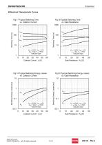
RGW60TS65CHR lElectrical Characteristic Curves Fig.18 Typical Switching Time vs. Gate Resistance 1000 Fig.17 Typical Switching Time vs. Collector Current 1000 Fig.20 Typocal Switching Energy Losses vs. Gate Resistance 10 Switching Energy Losses [mJ] Fig.19 Typical Switching Energy Losses vs. Collector Current 10 Switching Energy Losses [mJ] www.rohm.com © 2021 ROHM Co., Ltd. All rights reserved.
Open the catalog to page 9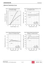
RGW60TS65CHR lElectrical Characteristic Curves Fig.21 Typical Diode Forward Current vs. Forward Voltage 100 Fig.22 Typical Diode Revese Recovery Time vs. Forward Current 50 Reverse Recovery Time : trr [ns] VCC = 400V diF/dt = 200A/μs Inductive load Fig.24 Typical Diode Rrverse Recovery Charge vs. Forward Current 70 Reverse Recovery Charge : Qrr [nC] Reverse Recovery Current : Irr [A] Fig.23 Typical Diode Reverse Recovery Current vs. Forward Current 5 VCC = 400V diF/dt = 200A/μs Inductive load 30 20 VCC = 400V diF/dt = 200A/μs Inductive load www.rohm.com © 2021 ROHM Co., Ltd. All rights reserved....
Open the catalog to page 10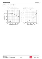
RGW60TS65CHR lElectrical Characteristic Curves Fig.25 Typical Diode Capacitance vs. Reverse Voltage Fig.26 Typical Diode Capacitance Store Energy 10 Capacitance Stored Energy : EC[mJ] www.rohm.com © 2021 ROHM Co., Ltd. All rights reserved.
Open the catalog to page 11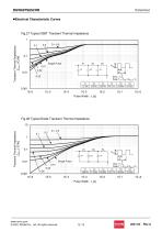
RGW60TS65CHR lElectrical Characteristic Curves Fig.27 Typical IGBT Transient Thermal Impedance Transient Thermal Impedance : Zθ(j-c) [°C/W] t1 t2 Duty = t1/t2 Peak Tj = PDM×Zθ(j-c)+TC Fig.28 Typical Diode Transient Thermal Impedance Transient Thermal Impedance : Zθ(j-c) [°C/W] 0.1 PDM t1 t2 Duty = t1/t2 Peak Tj = PDM×Zθ(j-c)+TC Single Pulse www.rohm.com © 2021 ROHM Co., Ltd. All rights reserved.
Open the catalog to page 12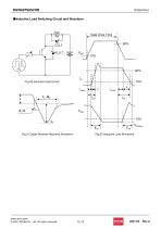
RGW60TS65CHR ●Inductive Load Switching Circuit and Waveform Gate Drive Time 90% Fig.29 Inductive Load Circuit td(off) toff Eon Fig.31 Diode Reverse Recovery Waveform www.rohm.com © 2021 ROHM Co., Ltd. All rights reserved. Fig.30 Inductive Load Waveform
Open the catalog to page 13All ROHM Semiconductor catalogs and technical brochures
 PSR series
17 Pages
 Microcontrollers
32 Pages
 Speech Synthesis LSI Series
20 Pages
 Next-Generation Op Amp series
12 Pages
 LED
LED18 Pages
 Diodes
30 Pages
 Intelligent Power Modules
3 Pages
 Full SiC Power Modules
3 Pages
 SiC Schottky Barrier Diodes
4 Pages
 Microcontroller
13 Pages
 Audio & Video
11 Pages
 Sensors & MEMS
4 Pages
 LED Drivers
4 Pages
 Power Management
36 Pages
 Data Converter
2 Pages
 Clocks & Timers
2 Pages
 Memory
6 Pages
 Motor Drivers
44 Pages
 Power Device Catalog
36 Pages
 CSL1501RW
9 Pages
 UT6JC5 -60V Pch+Pch Power MOSFET
14 Pages
 SH8JB5 -40V Pch+Pch Power MOSFET
14 Pages
 CSL1104WBx Series (x=A/B/C/D)
11 Pages
 BD9F500QUZ
58 Pages
 RGW00TS65CHR
15 Pages
 RGW80TS65CHR
15 Pages
 QH8KC5
14 Pages
 QH8KC6
14 Pages
 QH8KB5
14 Pages
 QH8KB6
14 Pages
 SH8KC6
14 Pages
 SH8KC7
14 Pages
 SH8KB6
14 Pages
 SH8KB7
14 Pages
 QH8MB5
22 Pages
 SH8MB5
22 Pages
 BM1390GLV-Z
31 Pages
 RPMD-0100
5 Pages
 Short Form Catalog
308 Pages
 EMARMOUR Technology
4 Pages
 Industrial Motor Solutions
40 Pages
 General-purpse ICs
40 Pages
 IPD
IPD4 Pages
 Quick Buck Booster®
6 Pages
 SOT-23 Package Products
4 Pages
 DC/DC Converter Selection Guide
40 Pages
 Linear Regulator Selection Guide
32 Pages
 Sensing Networks Catalog
11 Pages
 Power Solutions Catalog
9 Pages
 Power Management
11 Pages
 Motor Drivers
36 Pages
 Automotive Product Catalog
124 Pages
 EV solutions
8 Pages


Archived catalogs

- Single-pole switch
- Technology switch
- DC-DC converter
- Transistor module
- Industrial DC/DC converter module
- SMD DC-DC converter
- ERLO board-mount resistor
- ERLO power resistor
- Switching transistor
- High-speed diode
- Motor driver
- MOSFET transistor
- Power converter
- SMT diode
- Current rectifier
- Bipolar transistor
- ERLO thin-film resistor
- Switching DC-DC converter
- Step-down DC-DC converter